1 Introduction
This document describes how to implement a Radar Target Simulator/Generator using the Tabor Electronics’ Proteus AWT (Arbitrary Waveform Transceiver). The Proteus AWT RTS system is a configuration of the Proteus AWT that is design to receives a signal from the Radar under test and performs real time calculations in its internal FPGA to simulate a moving target.
For more information on Radar Signals, RF DAC and ADC Technology please review the documents listed in Section 4 of this solution note in advance of reading this note.
The following Proteus AWT’s are supported for this application:
Table 1‑1 Proteus Ordering Information
|
Model
|
Description
|
|
P1282B
|
1.25GS/s, 16Bit, AWG, 1GS Memory, 2CH, 4 Markers
|
|
P1284B
|
1.25GS/s, 16Bit, AWG, 1GS Memory, 4CH, 4 Markers
|
|
P1288B
|
1.25GS/s, 16Bit, 2GS Memory, 8CH 8 Markers
|
|
P12812B
|
1.25GS/s, 16Bit, 2GS Memory, 12CH 12 Markers
|
|
P2582B
|
2.5GS/s, 16Bit, 2GS Memory 2CH, 8 Markers
|
|
P2584B
|
2.5GS/s, 16Bit, 2GS Memory, 4CH, 8 Markers
|
|
P2588B
|
2.5GS/s, 16Bit, 2GS Memory, 8CH 16 Markers
|
|
P25812B
|
2.5GS/s, 16Bit, 2GS Memory, 12CH, 24 Markers
|
|
P9082B
|
9GS/s, 16Bit, 4GS Memory 2CH, 8 Markers
|
|
P9084B
|
9GS/s, 16Bit, 4GS Memory 4CH, 16 Markers
|
|
P9086B
|
9GS/s, 16Bit, 4GS Memory 6CH, 24 Markers
|
|
P9484D
|
9GS/s 16Bit 8GS Mem 4CH 8 Markers RF AWG Desktop
|
|
P9488D
|
9GS/s 16Bit 8GS Mem 8CH 16 Markers RF AWG Desktop
|
|
P94812D
|
9GS/s 16Bit 8GS Mem 12CH 24 Markers RF AWG Desktop
|
|
P9482M
|
9GS/s 16Bit 8GS Mem 2CH 8 Markers RF AWG Module
|
|
P9484M
|
9GS/s 16Bit 8GS Mem 4CH 8 Markers RF AWG Module
|
|
Mandatory Option
|
Description
|
|
AWT
|
5.4GS/s Single, 2.7GS/s Dual Channel 12 Bit Digitizer
|
|
PROG
|
High level FPGA programming capability through decision blocks of built-in Demodulation & digital Filters
|
Laboratory Workflow
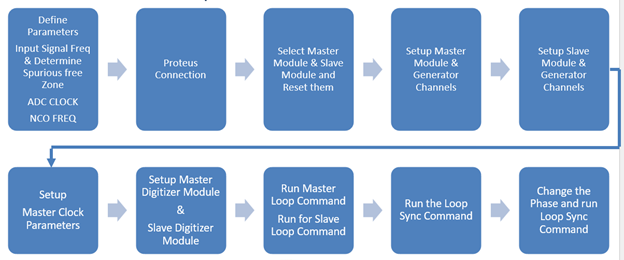
Figure 1.1 Flow Diagram of an 8-Channels Proteus RTS
- Setup a spurious free zone for the Proteus digitizer down converter (DDC). Refer to Figure 5 Excel Calculation for Proteus as RTS. You can use the Excel tool available for download from the Tabor web site.
- Apply the phase and amplitude settings to all Proteus output channels to form the beam for the required direction to simulate TDOA (Time Domain of Arrival). Refer to Figure 6 Output Channel and Digitizer Receiver Input Setups .
- Connect the Radar under test to the Proteus RF input SMA port. (ensure the signal has sufficient attenuation)
- Receive the signal and store it into the Proteus FPGA memory.
- Play the recorded data from the last sample depending on the requested loop delay. Refer to Table 3‑1 SCPI Command to Play Data with Delay.
- Transmit the same echo signal to all Proteus output channels.
- Connect the Proteus output channels to the radar under test (RUT).
- Please contact Tabor support to get the SCPI commands applicable for your device.
2 Radar Target Simulator Operation
The Tabor Proteus RTS/G works as a direct to RF/uW Digital RF Memory (DRFM), similar to many Commercial Off The Shelf) COTS cards, with the advantage of direct to RF DAC and ADC technology simplifying the block diagram, and easy configuration, programmability with a modular architecture that can expand its operation to multiple channels
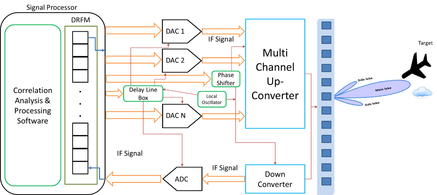
Figure 2.1 System Block Diagram for a Radar Target Simulator
Conceptually a RTS has both transmitting and receiving blocks. First the receiver will receive a signal from the radar under test. It is down-converted from RF (Radio Frequency) using a frequency conversion front end system to an IF (Intermediate Frequency) stage. The IF signal is digitized, demodulated and stored as IQ pairs in the FPGA RAM memory. The IQ samples are written sequentially starting from the first memory address. To creates a moving target simulation a delay is added between the received echo pulse while routing it back to the transmitter block. This delay can be accomplished by playing the samples starting from the last memory address to the first. The numbers of samples define the time delay of the pulse. After adding the delay to the baseband echo signal, it will pass through the DAC and will be up converted to the desired frequency of operation. Multiple DAC can be used to create a Mono-Pulse Simulation System, or an array of amplitude and phase weighted transmission elements could be used to create an electronically steered array.
3 Proteus as a Radar Target Simulator
Tabor Proteus AWT (Arbitrary Waveform Transceiver) series comes with an unique architecture of combination of AWG & Digitizer on a single FPGA. Similar to the block diagram of a DRFM system.
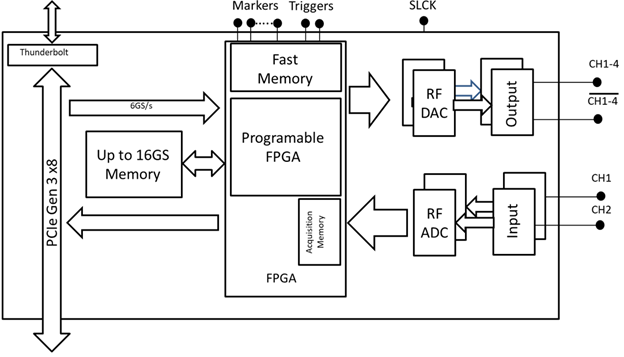
Figure 3.1 System Architecture of Proteus Series AWT (Arbitrary Waveform Transceiver)
Proteus Key Features
- Up to 4 channels and up to 9 GSa/s DAC sample rate
- Up to 16 bits DAC resolutions
- DUC/NCO mode for RF up conversion on all channels
- Skew between channels < 25ps
- Up to 2 digitizer channels per module
- Up to 5.4 GSa/s sample rate
- 12 bits ADC vertical resolution
- DDC mode for RF down-conversion on all channels
- Loopback mode
- Loop delay down to 400ns
- Direct streaming to DAC
- FPGA programming option
- FPGA shell option
3.1 Direct Generation of Complex RF Signals
Unlike many DRFM systems the Proteus series offers an integrated RF frequency conversion system. It uses a Numerically Controlled Oscillator (NCO), digital interpolator and IQ modulator to generate complex RF signals directly from the Proteus instrument. Direct generation of IQ signals from the DAC eliminates limitations such as IQ mismatch, and in-band carrier feed-through that are present with external IQ modulators and mixers. Also, by reducing the waveform size with up to x8 interpolation factor saves critical processing and compilation time that is present in many test and simulation systems.
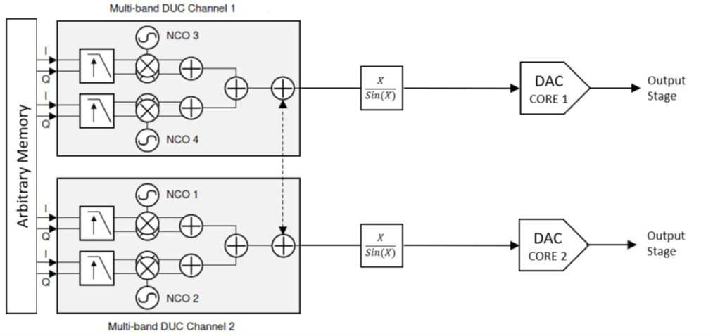
Figure 3.2 Proteus DUC Architecture
3.2 Ultra-Fast Communication Interface
The Proteus desktop platform offers an embedded PC with PCIe Gen3 x4 lanes interface as well as the fastest standardized communication interfaces commonly available in PCs today. These include USB3.0 and 10GbE interfaces as well as a Thunderbolt 3 interface, which enables up to 40Gb/s data transfer speed. For faster data conversion rates, the Proteus M family of PXIe cards with PCIe Geb 3 x8 lanes offers real-time data streaming at up to 5GS/s.
3.3 Feedback Control System
As the Proteus AWT integrates both DAC and ADC in one system, controlled by a single FPGA it provides high levels of synchronization with minimum latency. This high-speed internal control system allows for real-time modification of received radar signal, allowing for the emulation of moving targets.
3.4 Proteus RF AWT as RTS
Proteus series RF Arbitrary Waveform Transceivers are based on a modular format. Each module has 4 phase synchronous Direct to RF DAC channels enabled with DUC and 2 phase synchronous direct from RF ADC channels equipped with DDC features. Multiple modules can be used for more complex transmit receive configurations.
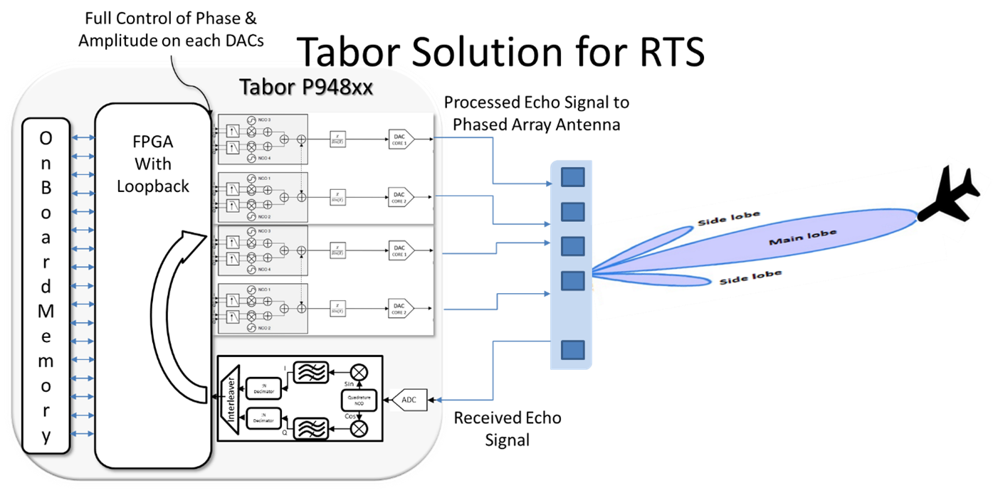
Figure 3.3 Proteus as RTS
Multiple Nyquist Zones can be used to transmit the signal at different carrier frequencies all the way to X-band. The amplitude and signal to noise ratio at the desired transmit frequency differs depending on the Nyquist Zone. The Desired frequency is a function of the clock frequency. For example, if the clock is 9GS/s and a 1GHz signal is negated the fundamental signal will appear at 1GHz, but we will also see images at 8GHz and 10GHz. (SCLK +/- Fundamental).
The ADC channels will receive the echo pulse reflected from the target and will pass through the DDC as shown in the above setup. This can operate in a different phase Nyquist zone. The ADC frequency response of the unit demonstrates good flatness across the analog bandwidth as shown in below figure.
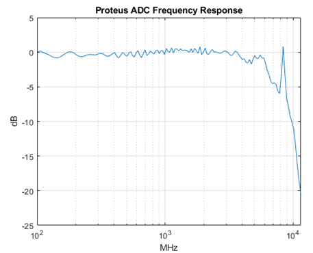
Figure 3.4 Proteus ADC Flatness
The DDC block (after the ADC in the above figure) will pass the IQ complex data to the FPGA that will store it in its memory. The FPGA will store the data starting from the first memory address. To get the required delay as explained previously it will play starting from the last memory address. Example code for this type of operation is as follow:
Table 3‑1 SCPI Command to Play Data with Delay
loopdelay = min(2047,loopdelay);
try
res = inst.SendScpi([':INST:ACT:SEL ' num2str(MODULE)]); % Select Master module
assert(res.ErrCode == 0);
% loop delay
res = inst.SendScpi([':DIG:LOOP:DELay ' num2str(loopdelay)]);
assert(res.ErrCode == 0);
%%%%%%%%%%%%%%%%%%%%%%%%%%%%%%%%%%%%%%%%%%%%%
res = inst.SendScpi([':INST:CHAN ' num2str(1)]);
assert(res.ErrCode == 0);
% scale and phase
res = inst.SendScpi([':DIG:LOOP:IQRotation ' num2str(SCALE) ',' num2str(CH1_PHASE)]);
assert(res.ErrCode == 0);
% Setup Amplitude
res = inst.SendScpi([':OUTP:VOLT ' num2str(CH1_AMPL)]);
assert(res.ErrCode == 0);
% loopback
res = inst.SendScpi(':DIG:LOOP ON');
assert(res.ErrCode == 0);
%%%%%%%%%%%%%%%%%%%%%%%%%%%%%%%%%%%%%%%%%%%%%
% Select the generator channel
res = inst.SendScpi([':INST:CHAN ' num2str(2)]);
assert(res.ErrCode == 0);
% scale and phase
res = inst.SendScpi([':DIG:LOOP:IQRotation ' num2str(SCALE) ',' num2str(CH2_PHASE)]);
assert(res.ErrCode == 0);
% Setup Amplitude
res = inst.SendScpi([':OUTP:VOLT ' num2str(CH2_AMPL)]);
assert(res.ErrCode == 0);
% loopback
res = inst.SendScpi(':DIG:LOOP ON');
assert(res.ErrCode == 0);
%%%%%%%%%%%%%%%%%%%%%%%%%%%%%%%%%%%%%%%%%%%%%
% Select the generator channel
res = inst.SendScpi([':INST:CHAN ' num2str(3)]);
assert(res.ErrCode == 0);
% scale and phase
res = inst.SendScpi([':DIG:LOOP:IQRotation ' num2str(SCALE) ',' num2str(CH3_PHASE)]);
assert(res.ErrCode == 0);
% Setup Amplitude
res = inst.SendScpi([':OUTP:VOLT ' num2str(CH3_AMPL)]);
assert(res.ErrCode == 0);
% loopback
res = inst.SendScpi(':DIG:LOOP ON');
assert(res.ErrCode == 0);
%%%%%%%%%%%%%%%%%%%%%%%%%%%%%%%%%%%%%%%%%%%%%
% Select the generator channel
res = inst.SendScpi([':INST:CHAN ' num2str(4)]);
assert(res.ErrCode == 0);
% scale and phase
res = inst.SendScpi([':DIG:LOOP:IQRotation ' num2str(SCALE) ',' num2str(CH4_PHASE)]);
assert(res.ErrCode == 0);
% Setup Amplitude
res = inst.SendScpi([':OUTP:VOLT ' num2str(CH4_AMPL)]);
assert(res.ErrCode == 0);
% loopback
res = inst.SendScpi(':DIG:LOOP ON');
assert(res.ErrCode == 0);
When transmitting the delayed signal, we need to ensure that none of the intermodulation products or harmonics fall in the range of the specified bandwidth and at carrier frequency. The Excel tool provided will help the user to configure the correct DDC NCO frequency.
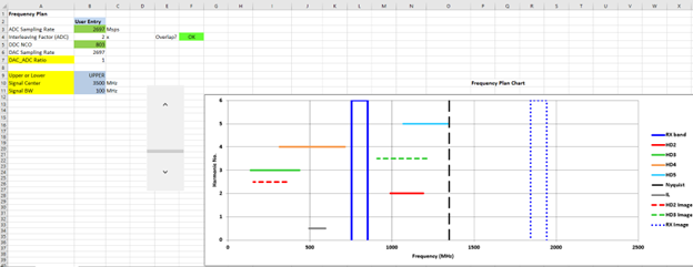
Figure 3.5 Excel Calculation for Proteus as RTS
As each module has four channels, each channel can employ phase and amplitude weighting to effectively steer the beam electronically.
Below shows the basic GUI for a single channel receiver and 4 channel transmitter.
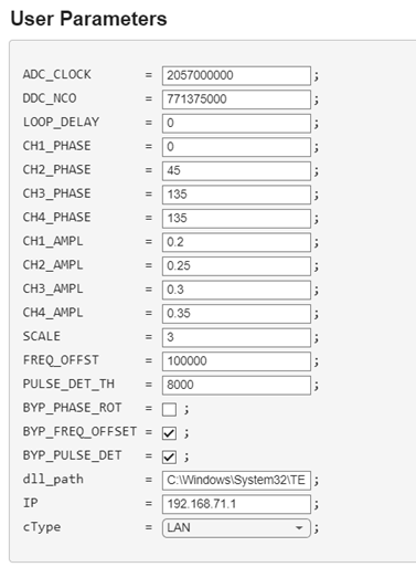
Figure 3.6 Output Channel and Digitizer Receiver Input Setups
Summary
The Proteus series of AWT’s have been designed to operate as both radar signal generation or simulation devices and with an optional digitizer to use as an analysis tool as well. Utilizing the built-in FPGA, full real-time loop back is also possible.
Standalone radar signal generator.
In loopback – Arbitrary Waveform Transceiver mode.
Streaming data directly to a DAC.
FPGA shell mode which gives the ability to customer configure the operation of the internal FPGA.
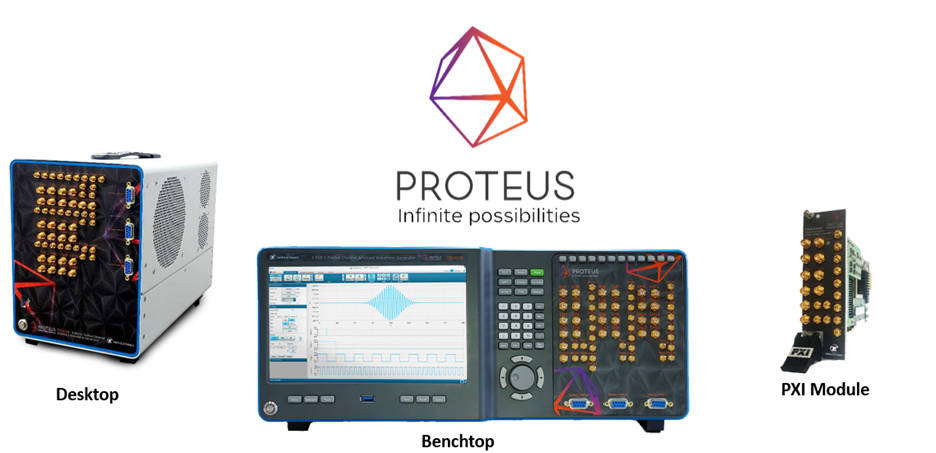
Figure 3.7 Proteus Family
4 More Information
For more information on microwave signal generation challenges and solutions, review the following resources on the Tabor web site (requires you to login to the site):
Stay Up To Date:
www.taborelec.com
LinkedIn page
YouTube channel
Corporate Headquarters
Address: 9 Hatasia St., 3688809 Nesher, Israel
Phone: (972) 4 8213393
Fax: (972) 4 8213388
For information: [email protected]
For service & support: [email protected]
US Sales & Support
Address: 1160 Battery Street #100, San Francisco, CA 94111
Phone: (628) 208 6418
For information: [email protected]
For service & support: [email protected]
India Sales & Support
Address: D-204, Sudarshan Pride, Ahmedabad 380060
Phone: (91) 90045 43308
For information [email protected]
For service & support [email protected]