Relevant Documents
 (218KB)
Background
Since the mid-1970s, the structural testing of loaded printed circuit boards (PCBs) has relied very heavily on the use of the so-called in-circuit “bed-of-nails” technique. This method of testing makes use of a fixture containing a bed-of-nails to access individual devices on the board through test landing sites or pads laid into the copper interconnect, or at other convenient contact points.
However, as technology progressed, the distance between interconnects decreased and multi-layer boards were introduced. As a result, the bed-of-nails no longer served as an effective solution for testing PCBs.
The situation was addressed by a group of test engineers from the Joint Test Action Group (JTAG), who defined a solution described in standard IEEE 1149.1. The standard describes the concept of a serial shift register around the boundary of the device. This concept became known as “Boundary Scan.” The boundary scan architecture provides a means to test interconnects without using physical test probes. It connects one or more so called Boundary Scan cells to each pin of the device that can selectively override the functionality of that pin.
Requirement
Boundary Scan cells can be programmed via the JTAG scan chain to drive a signal onto a pin and across an individual trace on the board. The cell at the destination of the board trace can then be programmed to read the value at the pin, verifying that the board trace properly connects the two pins.
The JTAG interface has a set of four dedicated test pins:
- Test Data In (TDI)
- Test Mode Select (TMS)
- Test Clock (TCK)
- Test Data Out (TDO)
Multiple chips on a board can have their JTAG lines daisy-chained together (see the image below), and a test probe need only connect to a single "JTAG port" to have access to all the chips on a circuit board.
JTAG testing equipment requires synchronized output channels that control the above mentioned test pins.
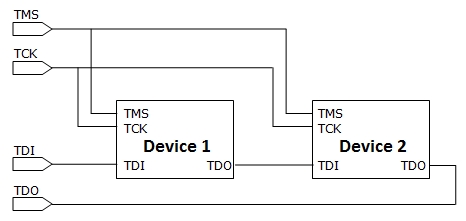
Figure 1: Daisy-Chained JTAG Lines
Solution
Tabor Electronics’ Wonder Wave family of Arbitrary Waveform Generators (AWGs) provides an ideal solution for JTAG Boundary Scan applications. Wonder Wave offers 4 synchronized output channels, supporting sampling rates of up to 200 MS/second, and is easily adapted for JTAG testing, as shown in Figure 2 below.
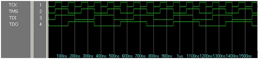
Figure 2: Wonder Wave Suport for JTAG Applications
Wonder Wave’s powerful sequence generator lets you link and loop segments in user-defined fashion, and stores up to 10 different sequence tables.
Wonder Wave is supplied with ArbConnection – Tabor’s comprehensive software tool that controls instrument operation, and provides unsurpassed programming and waveform creation capabilities. You can utilize ArbConnection’s Serial Data Composer to easily design waveforms for JTAG testing.
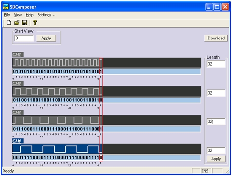
Figure 3: ArbConnection Serial Data Composer
For More Information
To learn more about Tabor’s solutions or to schedule a demo, please contact your local Tabor representative or email your request to [email protected]