The generation of complex RF signals require the simultaneous control of both the amplitude and phase of a carrier. One way to implement such control is an IQ modulator (Figure 1.1, a, left). There, the magnitude and phase instantaneous states are converted into a baseband complex modulating signal where the real part (or In-phase, I) modulates the amplitude of a carrier while the imaginary component (or quadrature, Q) is controls the amplitude of an orthogonal (p/2 phase) version of the same carrier before being added together. In traditional VSGs (Vector Signal Generators), an internal or external 2-channel AWG produces the baseband I/Q waveforms applied to the IQ modulator while an internal synthesizer produces the two orthogonal CW carriers applied to the I and Q modulators. Under this scheme, the sampling rate of the AWGs does not depend on the carrier frequency but on the modulation BW (Figure 1.1, a, right). Basically, sample rate for the AWGs must be equal or higher than the modulation bandwidth as the modulation bandwidth of a quadrature modulator is twice the bandwidth of the I and Q baseband signals. The accuracy and alignment of all the building blocks is extremely important, and their importance grows with the modulation bandwidth. Any difference in amplitude, frequency response, skew, sampling clock phase noise, etc. in the AWG will show up as a degraded quality RF signal. The same is true for the IQ modulator itself including the orthogonality of both carriers. It also applies to the L.O. synthesizer. All the linear or non-linear distortions can be measured through a single metrics such as the EVM (error vector magnitude), very popular in the wireless communication environment (Figure 1.1).
AWGs have been always part of any vector signal generation system as an internal or external component. In the figure below a) the traditional IQ generation scheme is shown. Two channels are used to generate the I and Q components to feed an IQ modulator. The required sampling rate for the AWG depends on the modulation bandwidth, not in the carrier frequency. In b), a single channel AWG is used to generate a modulated IF signal to feed a mixer. The mixer upconverts the IF signal to the final frequency. In this case, sampling rate is mainly determined by the IF carrier frequency. In both cases an additional L.O. source is required. When sampling rate is enough (so it is at least twice the carrier frequency) the final RF signal can be generated directly as seen in c) without the need for any external mixer, modulator or L.O: source. It is even possible to generate RF signals beyond the Nyquist frequency by using images of the signal located in higher order Nyquist bands as seen in d). Usually, a BPF (Bandpass Filter) is required to get rid of the unwanted images.
Another way to generate RF modulated waveforms is by using an AWG to produce a fully modulated IF signal with one single channel and then upconvert it to the final carrier frequency using an external mixer. Refer to Figure 1.1 b). This scheme requires an additional CW L.O. to feed the mixer. The advantage of this architecture is that the IQ modulation of the IF carrier is performed numerically when the waveform is calculated. As a result, there will not be I/Q alignment errors (amplitude, frequency response, skew, quadrature). The requirements for sampling rate will be higher, though. Sampling rate will have to be, at least, twice the maximum frequency component of the IF waveform. This means that the sampling frequency must be always higher than twice the carrier frequency and the modulation bandwidth.
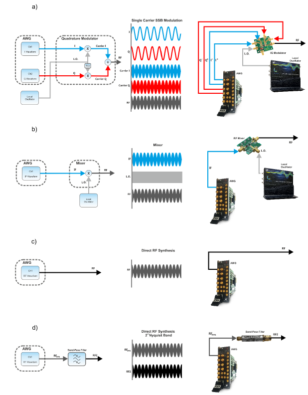
Figure 1.1 AWG Vector Signal Generation Methodologies
I/Q modulation is very sensitive to any inaccuracy affecting the I and Q components and the orthogonal fc carriers applied to them. A good way to visualize the influence of these inaccuracies is by applying two FM sinewaves with a 90O phase difference. The figure below depicts that in a perfect situation, the modulated I and Q components are added together in one of the fc±fm sidebands and are cancelled in the other (top left). If amplitudes of the I and Q components are not the same, cancellation is not perfect, and the Quadrature Imbalance impairment shows up (bottom left). If relative phase for carriers are not accurate, an unwanted residual sinewave shows-up resulting in the Quadrature Error impairment (top right). Finally, if some DC component is added to any of the modulating sinewaves or carriers, an unwanted residual carrier will appear (bottom right). This impairment is known as Carrier Leakage. In the real world there may be some other linear and non-linear impairments with similar effects. As any complex-modulated signal can be seen as the addition of infinite sinusoids, these impairments result in the signal interfering itself and reducing the signal-to-noise ratio. Identifying and measuring these impairments independently is necessary to apply corrections to reduce them. This can be quite difficult and time-consuming to do. Numerical quadrature modulation does not suffer this problem as all the components behave ideally.
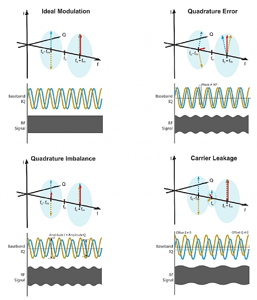
Figure 1.2 Ideal Modulation and Various Impairments
Any AWG can generate complex modulated IF/RF signals by just calculating the complete, modulated waveform and transferring it to the waveform memory. The sampling rate for the calculated and the generated waveforms will be the same and it is related to the carrier frequency.
The figure below depicts a different approach that is implementing in hardware a DUC (Digital Up-Converter) (here, a block diagram of the DUC implemented for each DAC in the Proteus series). The most important advantage consists in the fact that the waveform memory will store complex sample pairs (I/Q) that will be demultiplexed internally to two different multipliers where they will be combined with two orthogonal carriers generated by two NCOs set at the same frequency (fc) and 90O differential phase. As the I and Q waveforms are not related with the carrier frequency, these waveforms can be sampled at a sampling rate enough for the modulation bandwidth (basically sample rate >= modulation bandwidth). In order to match output sampling rate and the baseband waveforms sampling rate, an additional interpolation block must be added. In real DACs, interpolating factors are limited to a set of integer values so there is an integer relationship between the input and the output sampling rates. This scheme has several advantages as memory and calculation time is saved and the fc can be changed without having to recalculate the waveform, even on the fly.
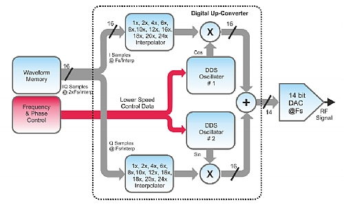
Figure 1.3 Proteus Block Diagram of the DUC Implemented for Each DAC
The figure below depicts that the capture of RF signals using a digitizer is quite symmetrical to the way AWG generate them with the signal flow going in the opposite direction. An external IQ demodulator can feed two digitizer channels (a), or a mixer can generate an IF signal at a lower frequency that can be digitized using one channel (b). If sampling rate and analog BW are enough, the RF signal can be directly captured in the first Nyquist zone of the digitizer (c) or in a higher order Nyquist band by under-sampling (d). In this case a BPF must be used to remove any signal located in the other Nyquist bands, if any.
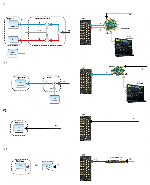
Figure 1.4 Capture of RF Signals Using a Digitizer
Eventually, if the sampling rate of the AWG is high enough, a modulated RF carrier can be generated directly (Figure 1.1, c). In this case, the requirements for the sampling rate will be even higher as the final carrier frequency will be higher than any IF frequency. It is true that ENoB (Effective Number of Bits) decrease as sampling rate grows, but the resulting quantization noise is spread over a wider BW, so the noise power density does not grow that much. When sampling rate is not enough for the target carrier frequency, an image located in a higher order Nyquist band can be used instead if the analog BW allows (Figure 1.1, d). AWGs such as the SE5082 incorporate DAC modes (RF mode) designed to minimize the amplitude of the image in the first Nyquist Band and emphasize the images in the second and third Nyquist band. Typically, a BPF is connected at the output to get rid of the undesired images. The main advantage of this RF generation scheme is the simplicity of it as no external devices (i.e. mixers, modulators, or L.O. sources) are necessary.
IF/RF direct generation requires higher sampling rates but less channels than baseband generation. It also requires higher sampling rates, and a higher sampling rate results in a larger waveform memory if the same time window must be generated. In order to ease those requirements, some RF-oriented AWGs, such as the Proteus family, incorporate an internal real-time I/Q modulator or DUC (Digital Up-Converter) (Figure 1.3). The beauty of real-time I/Q modulation is that it is associated to an ideal interpolation block so the I/Q sample pairs (now stored together and interleaved in the same waveform memory) are fed to the DAC block at a much lower sampling rate, defined by the modulation BW, so waveform memory and calculation and transfer time is greatly reduced. Additionally, the carrier frequency can be changed without modifying the I/Q waveform, just by setting the NCOs to the new frequency.
The same basic architectures can be also applied to the acquisition of modulated RF signals using DSOs or digitizers (Figure 1.4). In particular, it is possible to directly capture an RF signal even beyond the first Nyquist band by under-sampling the input signal if the analog BW of the digitizer is high enough. In order to do so, the center of the useful Nyquist band must be aligned with the RF signal to be captured by setting the appropriate sampling rate (Figure 1.5, a). Doing so, the waveform will show up as an image in the first Nyquist band. Depending on the Nyquist band being used, the spectrum of the image signal in the first Nyquist band will be reversed. Any other signal in any other Nyquist band will interfere with the target signal, so it may be necessary to apply a BPF to the input. The waveform can then be stored in the acquisition memory and further processed afterwards. Sampling rate and memory requirements for the acquisition are linked to the ADC sampling rate. However, the digitizer waveform could be processed in real-time through a DDC (Digital Down-Converter), an I/Q demodulator, figure 12b) to I/Q baseband and decimated so the final sampling rate is equal or higher than the modulation BW and not set by the carrier frequency. This operation also results in a “processing gain” (in effective bits) caused by the original oversampling respect to the one after decimation. A lower sampling rate results in lower waveform memory requirements and, even more importantly, faster waveform processing, a critical need for closed loop control.
The AWG section of the Proteus family is a good example of a direct-to-RF arbitrary waveform generation. All the Proteus models share the same DAC platform. However, the 1.25GSa/s and 2.5GSa/s maximum sample rate models can work in the 16-bit mode only. The 9GSa/s mode can still work in the 16-bit mode up to 2.5GSa/s but an additional working mode extend the sampling rate in direct conversion to 9GSa/s with 8-bit samples. Additionally, the 16-bit mode combined with the built-in real-time interpolation and DUC, allows for the generation of RF waveforms up to 7.5GHz (first and second Nyquist band) with high-resolution waveforms and excellent dynamic range and modulation bandwidth (>2GHz). Higher modulation bandwidths (>4GHz) can be still reached through the 8-bit mode. One of output stage options is especially designed for higher performance RF and mW signal generation. It removes any amplifier from the signal path, so linearity and bandwidth are improved. Additionally, it is AC-coupled as many RF devices are very sensitive to any remaining DC offset. SFDR (Spurious-Free Dynamic Range) specification offered by this option is excellent and can be >80dB over the full usable BW and even >90dB in the 1-2GHz range.
The Proteus DUC is a very flexible and powerful one. The DUC can be combined with the built-in interpolator so the waveform sampling rate can be adapted to the modulation BW rather than the carrier frequency. Interpolation factors supported are 2X, 4X, 6X, 8X, 10X, 12X, 16X, 18X, 20X, and 24X (Figure 1.6, a). Such flexible choice allows for an optimal effective sampling rate selection and the corresponding waveform memory savings. Interpolation, to be useful, must be combined with the application of a high-quality interpolation low-pass filter. The digital interpolation filters applied for every interpolation factor are excellent and show a 0.01dB ripple in the passband BW (0.4 X input waveform sampling rate) and a stopband attenuation higher than 90dB (Figure 1.6,b). NCOs are a very basic component of any DUC. Two NCOs working as a single quadrature oscillator are required for IQ modulation. The Proteus internal architecture allows for independent control of both frequency and phase for each 48-bit NCO in the IQ modulator. For regular IQ modulation, both NCOs share the same frequency while phase difference is set to 90o. Relative phase control is also possible between multiple channels in the same or multiple Proteus modules. This characteristic is paramount in any multiple RF channel generation application where carrier coherence is required. Phase-array radar, MIMO, and Qubit control are just some of these application areas.
The Proteus AWT digitizer section can work in two modes. In the basic mode all the channels can work up to 2.7GSa/s with 12 bits of vertical resolution. In the fast mode, every two channels can be combined to offer 5.4GSa/s sampling rate. Besides being usable as a regular digitizer from DC up to SR/2, it has been designed to be used as an IF/RF/mW acquisition system. Analog BW is excellent (>8GHz), and it can acquire bandwidth-limited signals (i.e. modulated carriers) in the second, third, and even the fourth Nyquist band. Supported modulation BW can reach > 1.3GHz for the basic mode and over 2.5GHz for the fast mode. The Proteus architecture also allows the implementation of additional waveform real-time processing implemented as standard blocks in the embedded FPGA. One of the blocks implemented is a DDC (or an I/Q demodulator). The DDC results in a stream of complex, baseband IQ samples that can be filtered and decimated based in the application needs. The sampling rate reduction results in an easier later processing and acquisition memory savings. The software trigger system can also trigger the acquisition based in the RF instantaneous power or RF pulse duration. Acquisitions can incorporate pre-trigger information and multiple frame time-stamped acquisitions with extremely low dead-time are possible. Data reduction can help in speeding up signal processing and even identification.
Figure below. In order to store and process an RF signal captured by a digitizer, it must be properly digitized. Waveforms captured by any ADC can be modelled as waveforms located in the first Nyquist band (DC-SR/2). When the analog BW of the ADC and the aperture time of the S/H circuit is small, any waveform fitting completely in any of the Nyquist band below the analog BW of the digitizer can be successfully captured as it was down-converted (a). Depending on the Nyquist band being used, the captured waveform will be reversed in the frequency domain. Any BW-limited signal in the first Nyquist band can be down-converted to complex baseband components (IQ) by applying a DDC (Digital Down Converter). Again, the DDC block diagram is very similar to a DUC with the signals flowing in the opposite direction. Sampling rate can be reduced (by decimation) according to the modulation bandwidth of the signal. Reducing the sampling rate improves waveform storage requirements and signal processing. The below figure shows how a 6.25GHz signal ca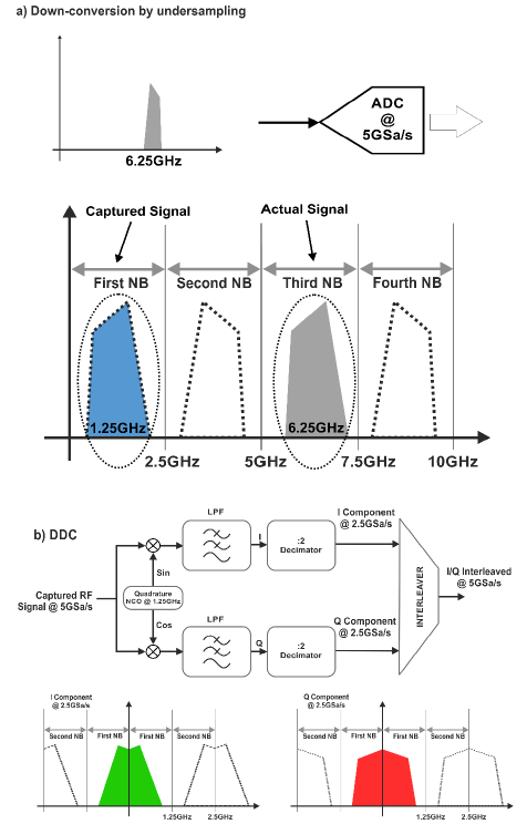 n be captured by a 5GSa/s digitizer with more than 2GHz Analysis Bandwidth.
Figure 1.5 Capture of RF Signals Using the Proteus Digitizer
The figure below depicts the DUC implemented in the Proteus DACs that is extremely powerful and flexible. One of the advantages of the architecture is that the initial phase for all of the NCOs in the different DACs can be set independent and coherently so the relative phase of all the carriers can be controlled. The FPGA can incorporate standard blocks for real and complex signal real-time corrections so modulated signals can be corrected for any carrier frequency (a). A critical component of any DUC is the interpolator (b). In the Proteus DACs the interpolator is composed by a zero-padding block and an interpolation/antialiasing filter. This filter is different for each interpolation factor. They are designed in such a way that they show near-perfect flatness for frequencies up to 0.4xfbb (sampling rate for the baseband components) and a >90 dB rejection for frequencies > fbb/2.
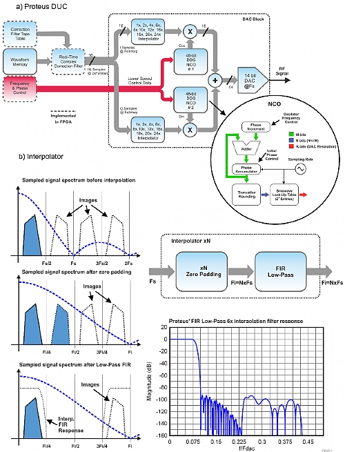
Figure 1.6 DUC Implementation in Proteus
Part 3 - High-Precision Waveform Generation and Acquisition
For more information contact [email protected]