New trends in RF/µW signal generation and acquisition and real-time closed-loop control for classical to quantum computing interfacing. The Classical/Quantum Interface in the figure below is implemented by the Proteus AWT (Arbitrary Waveform Transceiver). The figure below depicts how the Proteus AWT can be used to control multiple Qubits in an operational Quantum Computing system.
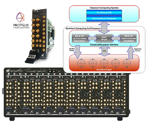
Figure 1.1 Proteus AWT Usage in a Quantum Computing System
1.1 From the “Proof Of Concept” Experiment to the Fully Functional Quantum Computer
In the past, most experiments related with quantum computing did not have the goal of performing actual computations. They were basically “proof-of-concept” experiments applied to the research of materials and architectures for Qubits (quantum bits) and the best way to control and capture their quantum state, implement quantum gates, and validate their operational principles. The qubit control devices of choice to implement such research systems were traditional, high-performance, T&M (Test and Measurement) lab equipment controlled from a classical computer through established communication interfaces and control protocols (Figure 1.2). In quantum computing research systems, several AWGs (Arbitrary Waveform Generators) are used to produce the quantum state control and reading signals combined with some digitizers or real-time DSOs (Digital Storage Oscilloscope) to capture the state of the qubits. Most AWGs and digitizers cannot cope with the frequencies of the control and state-readout signals. Those typically consists in some sort of microwave carrier modulated by some sequence of near-gaussian pulses in amplitude and phase (Figure 1.2, Figure 1.3). Instead of directly generating or capturing such signals, AWGs and DSOs must be combined with some mixers, IQ (In-phase Quadrature) modulators, amplifiers and filters (Figure 1.5). Mixers and IQ modulators require additional microwave LO (Local Oscillator) generators (i.e. CW microwave generators). Additional control signals, analog and digital, are also required. As a result, the cost per qubit was high while the scalability of the system was limited to a few Qubits.
The figure below depicts how T&M equipment have been extensively used to control and measure Qubits in experimental QC (Quantum Computing) systems. Traditional Rack&Stack instrumentation is the most popular given the level of performance and flexibility. In these experimental systems, multiple multichannel AWGs combined with additional IQ modulators and mixers are applied to the quantum layer, while Vector Spectrum Analyzers or high-bandwidth real-time digital oscilloscopes are used to read the state of the Qubits. Very complex and fast sequences of stimuli and responses can be executed thanks to the powerful triggering and sequencing capabilities of modern instruments. However, the genuine real-time close-loop control required for actual, practical quantum computing cannot be implemented given the speed limitations of the control system and the communication buses.
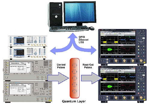
Figure 1.2 Proof-of-Concept Quantum Computer Experiment
The figures below depict the way the quantum state of qubits can be controlled and captured is different for each technology and implementation. Here, two different sets of control (green) and read-out (red) RF pulses are shown for two different qubit technologies, Rabi Oscillation (Figure 1.3) and Spin Echo (Figure 1.4). They share some characteristics, though. The shape, timing, RF/µW carrier frequency and phase must be tightly controlled and may be different for each step and each pulse. Generating this kind of signals using traditional AWGs would require 4 or more channel per qubit in addition to several external IQ (In-phase Quadrature) modulators and mixers. In real quantum computing systems, the characteristics (shape, timing) of the control pulses for each step depend on the states read after the execution of the current state and it must be analysed and set in a matter of hundreds of ns.
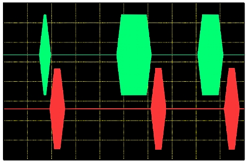
Figure 1.3 Rabi Oscillation Qubit Technology
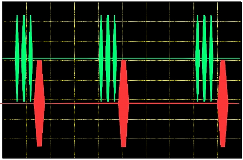
Figure 1.4 Spin Echo Qubit Technology
The figure below depicts the traditional approach to generate RF pulses using an AWG is either by generating the (I/Q) baseband signals and an additional I/Q modulator, or by generating a modulated IF signal and the upconvert it to the final frequency by using a mixer. Here a Tabor Proteus P9082M, 2-channel, 9GSa/s AWG is being used to generate 2 tones around 6GHz and using either a mixer (shown connected) or an IQ modulator (the 4-port module at the left of the mixer). A Tabor LS1291D 12GHz analog RF signal generator is used as the L.O. required for the mixer and the I/Q modulator. Results can be seen in the column in the right. The SA (Spectrum Analyzer) capture in the center corresponds to the I/Q modulator which required two AWG channels. The unwanted tone in the middle of the two wanted tones results from a typical impairment in IQ modulators, carrier feed-through. There are many other impairments and aligning IQ modulators is difficult and time consuming. The capture at the bottom corresponds to the same signal using an IF (Intermediate Frequency) generated by one channel. In this case, the IF carrier frequency is around 1GHz (shown at the top capture). As the modulation of the IF carrier has been performed numerically using a single channel, there are not impairments caused by the modulation process itself and, therefore, no carrier feedthrough is visible in the Spectrum. With this particular AWG, the carrier frequency could be set to 6GHz directly so the mixer could be made redundant (photo and measurements courtesy of Mark Elo, Tabor Electronics, and Charles Greenberg, Astronics).
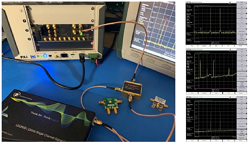
Figure 1.5 Using a Mixer to Up-Convert a Proteus-Generated IF Signal
The main reason why actual computing was not possible through this kind of “scenario-oriented” approach was the speed required to perform a significant number of “feed-back/ forward” cycles in the available coherence time (survival period of superposition and entanglement for the Qubits in the system). This is especially critical for superconducting qubits where coherence time may be just a few hundreds of microseconds. This requirement results in the need of being capable of perform a single “feedback/forward” cycle in a period ranging from a few hundreds of nanoseconds up to a few microseconds. These speed requirements cannot be handled in real-time by traditional T&M instrumentation and the associated classical computing control systems. Instead, in those systems, the sequence of quantum states is predefined so AWGs apply sequentially the corresponding control and read-out signals while DSOs and digitizers capture the resulting quantum states of the qubits so their correctness and reliability can be established. In a real quantum computer, the next quantum state of the qubits depends on their previous quantum states according to the quantum gates applied sequentially according to the quantum algorithm being executed. In order to fulfill this requirement at speeds compatible with the actual coherence time supported by the qubit technology being used, a very fast closed-loop control system capable to read the quantum states from the different qubits, apply the quantum gates for the current step in the algorithm, and set the new states for all the qubits in the quantum computer (Figure 1.6). Given the number of qubits involved in working quantum computer and the number of signals to handle, it is virtually impossible to implement such classical to quantum computing interface using traditional T&M equipment under the control of a single computer. These speed (and reasonable cost) requirements can be only met by implementing a distributed real-time closed-loop control system based total or partially in hardware tightly connected to the waveform generation and capture blocks. Under this scheme, an FPGA or ASIC connected to high-speed DACs and ADCs controls one or a few qubits while it communicates at high speed with the other closed-loop control blocks in the system.
Any quantum bit control system is extremely sensitive to noise. In addition to traditional thermal noise, crosstalk or quantization error, any deviation of the waveforms applied to or read from qubits respect to the ideal ones can look as noise added to the system. Noise will result in higher computational errors or even system decoherence. Linear and non-linear distortions added by the signal generation and capture chains result in such deviation, thus increasing noise. System characterization, calibration and correction is paramount for a successful implementation.
The figure below depicts an Operating Quantum Computing system that can be described as a classical computer connected to a quantum computing coprocessor through a Classical/Quantum interfacing block. This block must implement multiple analog (both baseband and RF) and digital input and output channels and it must take control of the feedback-forward cycles according to the quantum algorithm being executed. As the processing speed requirements are high and the processing power required grows with the number of Qubits, the ideal implementation should incorporate multiple fast signals processors in the loop. In this way, the classical computer only sets-up the computing sequence, monitors the execution of the algorithm, and reads and validates the results. Using specific, scalable HW in the control loop is the best way to reach the level of performance required and this is possible through the usage of application-specific IC (ASIC) or field-programmable gate arrays (FPGA). The Proteus series of Arbitrary Waveform Transceiver implements most (if not all) the Classical/Quantum Interface by providing all the blocks shown and incorporating an FPGA fully accessible to users.
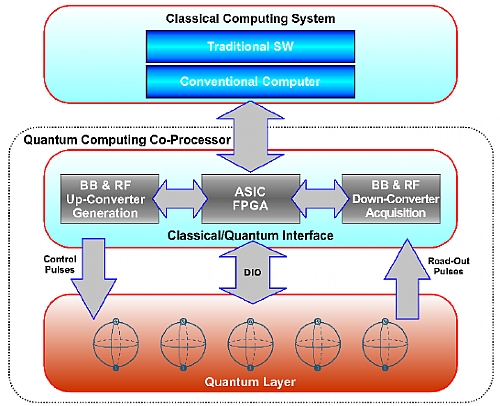
Figure 1.6 Block Diagram of an Operating Quantum Computing System
1.2 Proteus Designed for Quantum Computing
During the past years, Tabor Electronics has been one of the leading suppliers of high-performance AWGs for the Quantum Computing research community. In particular, the SE5082 AWG (Figure 1.7), with its two 5GSa/s (5Gigasamples/second) channels and extremely high analog BW (Band Width), especial RF (Radio Frequency) working modes to efficiently produce signals in the second and third Nyquist bands, and advanced sequencing, has been extensively used in the field of Quantum Computing research. The compact size and low cost per channel of the SE5082 makes it extremely attractive for QC researchers to be applied to “proof-of-concept” research devices.
The figure below depicts the Tabor SE5082, 2-channel, 5GSa/s AWG that have been used extensively in the quantum computing application area. It is ideal to generate IF and RF signals directly as its analog BW and different DAC (Digital to Analog Converter) operating modes allow for the generation of complex modulated RF signals in the second and third Nyquist band, well beyond 7GHz. The Tabor WX series of AWGs, with up to four channels at 2.3GSa/s have been also widely used in the quantum computing research field projects.
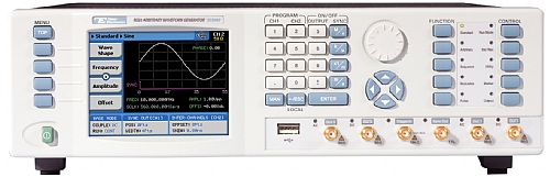
Figure 1.7 SE5082, 2-channel, 5GSa/s AWG
Tabor Electronics have gathered all the feed-back from QC users to define the next generation of products; the Proteus family of AWG and AWT (Arbitrary Waveform Transceiver, figure 6). Available in different form factors (PXI modular, desktop, and benchtop) and sampling rates (1.25GSa/s, 2.5Gsa/s and 9Gsa/s) with an usable analog BW close to 8GHz, all the components of the family share the same basic compact, high-density architecture, offering up to 4 16-bit AWG channels in a 2-slot PXI module or up to 12 AWG channels in a single desktop or benchtop system. Waveform memory size is huge (up to 16GSamples) and memory segmentation and advanced sequencing (including conditional branching) can support the most extreme synchronized waveform generation scenarios.
However, although impressive, the AWG performance is not the only appealing characteristic of the Proteus solution for quantum computer researchers and designers. It is the built-in capability of closing the loop and implement “feedback-forward” cycles at the right speed what allows operational quantum computers to work. And this is possible for two reasons. First, the Proteus family creates a new product category, the AWT (Arbitrary Waveform Transceiver), by incorporating a two-channel 12-bit digitizer per PXI module (up to 4 channels per desktop or benchtop system) running at up to 5.4GSa/s with enough analog BW to digitize signals up to 9GHz. The second reason is the availability of a high-speed FPGA (Field Programmable Gate Array) (Xilinx UltraScale KU-060) that is open for users to be programmed. This FPGA is directly connected to the analog outputs (AWG) and inputs (digitizer), the DDR4 massive memory, multiple digital 1.25 Gbps digital input/outputs (8 markers and 2 GPIO) and the PCIe Gen3, 8-lanes backplane capable of supporting sustained communication at 50Gb/s (Figure 1.10).
The new Tabor Proteus series of Arbitrary Waveform Transceivers is designed to match the requirements of Quantum Computer designers. It combines analog and digital high-speed inputs and outputs in the same platform along with a user-accessible FPGA for applications required closed-loop and real-time signal processing. The PXI modules (Figure 1.8) can incorporate up to 4 channels of AWG (1.25, 2.5, or 9GSa/s) and 2 digitizer channels (2.7 or 5.4 GSa/s) with up to 10 digital input/outputs (1.25gbps) in a single 2 o 3-slot PXI module. The benchtop models (Figure 1.9) can incorporate up to 12 channels of AWG and up to 4 digitizer channels in a single device. Multiple modules and devices can operate synchronously without the need for additional synchronization hardware.
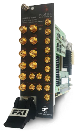
Figure 1.8 Proteus PXI Module
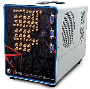
Figure 1.9 Proteus Desktop Model
Both the AWG and digitizer blocks have been designed to directly generate and capture RF and microwave signals. Analog output channels incorporate internal numerical IQ modulators and upconverters (DUC Digital Up-Converter) while analog input channels can incorporate digital down converters and demodulators as standard processing blocks in the FPGA. RF quality of the signals in excellent regarding SFDR (Spurious Free Dynamic Range) and phase noise.
The block diagram below is for a Proteus PXI AWT module that is very similar to the one for the Classical/Quantum Computing Interface shown in Figure 1.6. Both the inputs and outputs can be used to the acquisition and generation of baseband (DC to Sample Rate /2) and RF over multiple Nyquist Bands up to 8GHz. A great portion of the gates in the Xilinx Kintex© FPGA are free to use so any application-specific closed loop control and/or signal processing application can be implemented. The massive DDR4 memory is capable of storing up to 16GSamples while the PCIe Gen.3, 8 lanes bus can handle continuous streaming from the digitizer or to the AWG at sampling rates beyond 6GSa/s. The same bus allows for the fast interconnection of multiple modules.
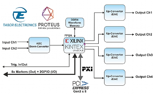
Figure 1.10 Proteus AWT Block Diagram
Part 2 - Direct to Microwave Signal Generation and Acquisition
For more information contact [email protected]