Relevant Documents
 (2862KB)
1 A New Paradigm for the Classical to Quantum Computing Interface
New trends in RF/µW signal generation and acquisition and real-time closed-loop control for classical to quantum computing interfacing. The Classical/Quantum Interface in the figure below is implemented by the Proteus AWT (Arbitrary Waveform Transceiver). The figure below depicts how the Proteus AWT can be used to control multiple Qubits in an operational Quantum Computing system.
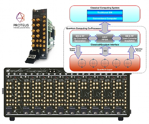
Figure 1.1 Proteus AWT Usage in a Quantum Computing System
1.1 From the “Proof Of Concept” Experiment to the Fully Functional Quantum Computer
In the past, most experiments related with quantum computing did not have the goal of performing actual computations. They were basically “proof-of-concept” experiments applied to the research of materials and architectures for Qubits (quantum bits) and the best way to control and capture their quantum state, implement quantum gates, and validate their operational principles. The qubit control devices of choice to implement such research systems were traditional, high-performance, T&M (Test and Measurement) lab equipment controlled from a classical computer through established communication interfaces and control protocols (Figure 1.2). In quantum computing research systems, several AWGs (Arbitrary Waveform Generators) are used to produce the quantum state control and reading signals combined with some digitizers or real-time DSOs (Digital Storage Oscilloscope) to capture the state of the qubits. Most AWGs and digitizers cannot cope with the frequencies of the control and state-readout signals. Those typically consists in some sort of microwave carrier modulated by some sequence of near-gaussian pulses in amplitude and phase (Figure 1.2, Figure 1.3). Instead of directly generating or capturing such signals, AWGs and DSOs must be combined with some mixers, IQ (In-phase Quadrature) modulators, amplifiers and filters (Figure 1.5). Mixers and IQ modulators require additional microwave LO (Local Oscillator) generators (i.e. CW microwave generators). Additional control signals, analog and digital, are also required. As a result, the cost per qubit was high while the scalability of the system was limited to a few Qubits.
The figure below depicts how T&M equipment have been extensively used to control and measure Qubits in experimental QC (Quantum Computing) systems. Traditional Rack&Stack instrumentation is the most popular given the level of performance and flexibility. In these experimental systems, multiple multichannel AWGs combined with additional IQ modulators and mixers are applied to the quantum layer, while Vector Spectrum Analyzers or high-bandwidth real-time digital oscilloscopes are used to read the state of the Qubits. Very complex and fast sequences of stimuli and responses can be executed thanks to the powerful triggering and sequencing capabilities of modern instruments. However, the genuine real-time close-loop control required for actual, practical quantum computing cannot be implemented given the speed limitations of the control system and the communication buses.
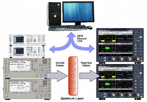
Figure 1.2 Proof-of-Concept Quantum Computer Experiment
The figures below depict the way the quantum state of qubits can be controlled and captured is different for each technology and implementation. Here, two different sets of control (green) and read-out (red) RF pulses are shown for two different qubit technologies, Rabi Oscillation (Figure 1.3) and Spin Echo (Figure 1.4). They share some characteristics, though. The shape, timing, RF/µW carrier frequency and phase must be tightly controlled and may be different for each step and each pulse. Generating this kind of signals using traditional AWGs would require 4 or more channel per qubit in addition to several external IQ (In-phase Quadrature) modulators and mixers. In real quantum computing systems, the characteristics (shape, timing) of the control pulses for each step depend on the states read after the execution of the current state and it must be analysed and set in a matter of hundreds of ns.
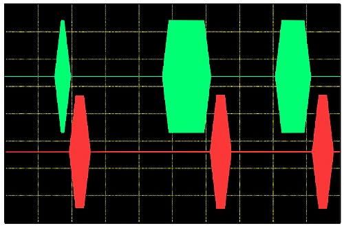
Figure 1.3 Rabi Oscillation Qubit Technology
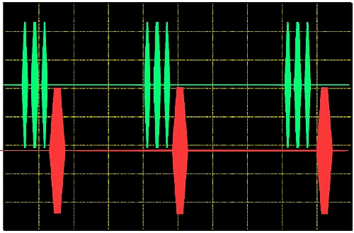
Figure 1.4 Spin Echo Qubit Technology
The figure below depicts the traditional approach to generate RF pulses using an AWG is either by generating the (I/Q) baseband signals and an additional I/Q modulator, or by generating a modulated IF signal and the upconvert it to the final frequency by using a mixer. Here a Tabor Proteus P9082M, 2-channel, 9GSa/s AWG is being used to generate 2 tones around 6GHz and using either a mixer (shown connected) or an IQ modulator (the 4-port module at the left of the mixer). A Tabor LS1291D 12GHz analog RF signal generator is used as the L.O. required for the mixer and the I/Q modulator. Results can be seen in the column in the right. The SA (Spectrum Analyzer) capture in the center corresponds to the I/Q modulator which required two AWG channels. The unwanted tone in the middle of the two wanted tones results from a typical impairment in IQ modulators, carrier feed-through. There are many other impairments and aligning IQ modulators is difficult and time consuming. The capture at the bottom corresponds to the same signal using an IF (Intermediate Frequency) generated by one channel. In this case, the IF carrier frequency is around 1GHz (shown at the top capture). As the modulation of the IF carrier has been performed numerically using a single channel, there are not impairments caused by the modulation process itself and, therefore, no carrier feedthrough is visible in the Spectrum. With this particular AWG, the carrier frequency could be set to 6GHz directly so the mixer could be made redundant (photo and measurements courtesy of Mark Elo, Tabor Electronics, and Charles Greenberg, Astronics).
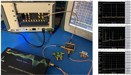
Figure 1.5 Using a Mixer to Up-Convert a Proteus-Generated IF Signal
The main reason why actual computing was not possible through this kind of “scenario-oriented” approach was the speed required to perform a significant number of “feed-back/ forward” cycles in the available coherence time (survival period of superposition and entanglement for the Qubits in the system). This is especially critical for superconducting qubits where coherence time may be just a few hundreds of microseconds. This requirement results in the need of being capable of perform a single “feedback/forward” cycle in a period ranging from a few hundreds of nanoseconds up to a few microseconds. These speed requirements cannot be handled in real-time by traditional T&M instrumentation and the associated classical computing control systems. Instead, in those systems, the sequence of quantum states is predefined so AWGs apply sequentially the corresponding control and read-out signals while DSOs and digitizers capture the resulting quantum states of the qubits so their correctness and reliability can be established. In a real quantum computer, the next quantum state of the qubits depends on their previous quantum states according to the quantum gates applied sequentially according to the quantum algorithm being executed. In order to fulfill this requirement at speeds compatible with the actual coherence time supported by the qubit technology being used, a very fast closed-loop control system capable to read the quantum states from the different qubits, apply the quantum gates for the current step in the algorithm, and set the new states for all the qubits in the quantum computer (Figure 1.6). Given the number of qubits involved in working quantum computer and the number of signals to handle, it is virtually impossible to implement such classical to quantum computing interface using traditional T&M equipment under the control of a single computer. These speed (and reasonable cost) requirements can be only met by implementing a distributed real-time closed-loop control system based total or partially in hardware tightly connected to the waveform generation and capture blocks. Under this scheme, an FPGA or ASIC connected to high-speed DACs and ADCs controls one or a few qubits while it communicates at high speed with the other closed-loop control blocks in the system.
Any quantum bit control system is extremely sensitive to noise. In addition to traditional thermal noise, crosstalk or quantization error, any deviation of the waveforms applied to or read from qubits respect to the ideal ones can look as noise added to the system. Noise will result in higher computational errors or even system decoherence. Linear and non-linear distortions added by the signal generation and capture chains result in such deviation, thus increasing noise. System characterization, calibration and correction is paramount for a successful implementation.
The figure below depicts an Operating Quantum Computing system that can be described as a classical computer connected to a quantum computing coprocessor through a Classical/Quantum interfacing block. This block must implement multiple analog (both baseband and RF) and digital input and output channels and it must take control of the feedback-forward cycles according to the quantum algorithm being executed. As the processing speed requirements are high and the processing power required grows with the number of Qubits, the ideal implementation should incorporate multiple fast signals processors in the loop. In this way, the classical computer only sets-up the computing sequence, monitors the execution of the algorithm, and reads and validates the results. Using specific, scalable HW in the control loop is the best way to reach the level of performance required and this is possible through the usage of application-specific IC (ASIC) or field-programmable gate arrays (FPGA). The Proteus series of Arbitrary Waveform Transceiver implements most (if not all) the Classical/Quantum Interface by providing all the blocks shown and incorporating an FPGA fully accessible to users.
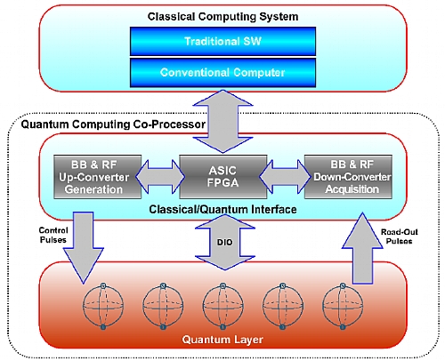
Figure 1.6 Block Diagram of an Operating Quantum Computing System
1.2 Proteus Designed for Quantum Computing
During the past years, Tabor Electronics has been one of the leading suppliers of high-performance AWGs for the Quantum Computing research community. In particular, the SE5082 AWG (Figure 1.7), with its two 5GSa/s (5Gigasamples/second) channels and extremely high analog BW (Band Width), especial RF (Radio Frequency) working modes to efficiently produce signals in the second and third Nyquist bands, and advanced sequencing, has been extensively used in the field of Quantum Computing research. The compact size and low cost per channel of the SE5082 makes it extremely attractive for QC researchers to be applied to “proof-of-concept” research devices.
The figure below depicts the Tabor SE5082, 2-channel, 5GSa/s AWG that have been used extensively in the quantum computing application area. It is ideal to generate IF and RF signals directly as its analog BW and different DAC (Digital to Analog Converter) operating modes allow for the generation of complex modulated RF signals in the second and third Nyquist band, well beyond 7GHz. The Tabor WX series of AWGs, with up to four channels at 2.3GSa/s have been also widely used in the quantum computing research field projects.
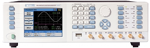
Figure 1.7 SE5082, 2-channel, 5GSa/s AWG
Tabor Electronics have gathered all the feed-back from QC users to define the next generation of products; the Proteus family of AWG and AWT (Arbitrary Waveform Transceiver, figure 6). Available in different form factors (PXI modular, desktop, and benchtop) and sampling rates (1.25GSa/s, 2.5Gsa/s and 9Gsa/s) with an usable analog BW close to 8GHz, all the components of the family share the same basic compact, high-density architecture, offering up to 4 16-bit AWG channels in a 2-slot PXI module or up to 12 AWG channels in a single desktop or benchtop system. Waveform memory size is huge (up to 16GSamples) and memory segmentation and advanced sequencing (including conditional branching) can support the most extreme synchronized waveform generation scenarios.
However, although impressive, the AWG performance is not the only appealing characteristic of the Proteus solution for quantum computer researchers and designers. It is the built-in capability of closing the loop and implement “feedback-forward” cycles at the right speed what allows operational quantum computers to work. And this is possible for two reasons. First, the Proteus family creates a new product category, the AWT (Arbitrary Waveform Transceiver), by incorporating a two-channel 12-bit digitizer per PXI module (up to 4 channels per desktop or benchtop system) running at up to 5.4GSa/s with enough analog BW to digitize signals up to 9GHz. The second reason is the availability of a high-speed FPGA (Field Programmable Gate Array) (Xilinx UltraScale KU-060) that is open for users to be programmed. This FPGA is directly connected to the analog outputs (AWG) and inputs (digitizer), the DDR4 massive memory, multiple digital 1.25 Gbps digital input/outputs (8 markers and 2 GPIO) and the PCIe Gen3, 8-lanes backplane capable of supporting sustained communication at 50Gb/s (Figure 1.10).
The new Tabor Proteus series of Arbitrary Waveform Transceivers is designed to match the requirements of Quantum Computer designers. It combines analog and digital high-speed inputs and outputs in the same platform along with a user-accessible FPGA for applications required closed-loop and real-time signal processing. The PXI modules (Figure 1.8) can incorporate up to 4 channels of AWG (1.25, 2.5, or 9GSa/s) and 2 digitizer channels (2.7 or 5.4 GSa/s) with up to 10 digital input/outputs (1.25gbps) in a single 2 o 3-slot PXI module. The benchtop models (Figure 1.9) can incorporate up to 12 channels of AWG and up to 4 digitizer channels in a single device. Multiple modules and devices can operate synchronously without the need for additional synchronization hardware.
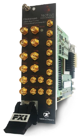
Figure 1.8 Proteus PXI Module
Figure 1.9 Proteus Desktop Model
Both the AWG and digitizer blocks have been designed to directly generate and capture RF and microwave signals. Analog output channels incorporate internal numerical IQ modulators and upconverters (DUC Digital Up-Converter) while analog input channels can incorporate digital down converters and demodulators as standard processing blocks in the FPGA. RF quality of the signals in excellent regarding SFDR (Spurious Free Dynamic Range) and phase noise.
The block diagram below is for a Proteus PXI AWT module that is very similar to the one for the Classical/Quantum Computing Interface shown in Figure 1.6. Both the inputs and outputs can be used to the acquisition and generation of baseband (DC to Sample Rate /2) and RF over multiple Nyquist Bands up to 8GHz. A great portion of the gates in the Xilinx Kintex© FPGA are free to use so any application-specific closed loop control and/or signal processing application can be implemented. The massive DDR4 memory is capable of storing up to 16GSamples while the PCIe Gen.3, 8 lanes bus can handle continuous streaming from the digitizer or to the AWG at sampling rates beyond 6GSa/s. The same bus allows for the fast interconnection of multiple modules.
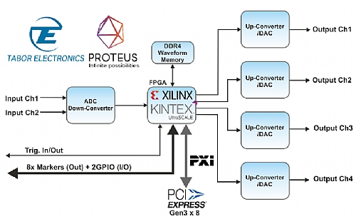
Figure 1.10 Proteus AWT Block Diagram
2 Direct to Microwave Signal Generation and Acquisition
The generation of complex RF signals require the simultaneous control of both the amplitude and phase of a carrier. One way to implement such control is an IQ modulator (Figure 2.1, a, left). There, the magnitude and phase instantaneous states are converted into a baseband complex modulating signal where the real part (or In-phase, I) modulates the amplitude of a carrier while the imaginary component (or quadrature, Q) is controls the amplitude of an orthogonal (p/2 phase) version of the same carrier before being added together. In traditional VSGs (Vector Signal Generators), an internal or external 2-channel AWG produces the baseband I/Q waveforms applied to the IQ modulator while an internal synthesizer produces the two orthogonal CW carriers applied to the I and Q modulators. Under this scheme, the sampling rate of the AWGs does not depend on the carrier frequency but on the modulation BW (Figure 2.1, a, right). Basically, sample rate for the AWGs must be equal or higher than the modulation bandwidth as the modulation bandwidth of a quadrature modulator is twice the bandwidth of the I and Q baseband signals. The accuracy and alignment of all the building blocks is extremely important, and their importance grows with the modulation bandwidth. Any difference in amplitude, frequency response, skew, sampling clock phase noise, etc. in the AWG will show up as a degraded quality RF signal. The same is true for the IQ modulator itself including the orthogonality of both carriers. It also applies to the L.O. synthesizer. All the linear or non-linear distortions can be measured through a single metrics such as the EVM (error vector magnitude), very popular in the wireless communication environment (Figure 2.1).
AWGs have been always part of any vector signal generation system as an internal or external component. In the figure below a) the traditional IQ generation scheme is shown. Two channels are used to generate the I and Q components to feed an IQ modulator. The required sampling rate for the AWG depends on the modulation bandwidth, not in the carrier frequency. In b), a single channel AWG is used to generate a modulated IF signal to feed a mixer. The mixer upconverts the IF signal to the final frequency. In this case, sampling rate is mainly determined by the IF carrier frequency. In both cases an additional L.O. source is required. When sampling rate is enough (so it is at least twice the carrier frequency) the final RF signal can be generated directly as seen in c) without the need for any external mixer, modulator or L.O: source. It is even possible to generate RF signals beyond the Nyquist frequency by using images of the signal located in higher order Nyquist bands as seen in d). Usually, a BPF (Bandpass Filter) is required to get rid of the unwanted images.
Another way to generate RF modulated waveforms is by using an AWG to produce a fully modulated IF signal with one single channel and then upconvert it to the final carrier frequency using an external mixer. Refer to Figure 2.1 b). This scheme requires an additional CW L.O. to feed the mixer. The advantage of this architecture is that the IQ modulation of the IF carrier is performed numerically when the waveform is calculated. As a result, there will not be I/Q alignment errors (amplitude, frequency response, skew, quadrature). The requirements for sampling rate will be higher, though. Sampling rate will have to be, at least, twice the maximum frequency component of the IF waveform. This means that the sampling frequency must be always higher than twice the carrier frequency and the modulation bandwidth.
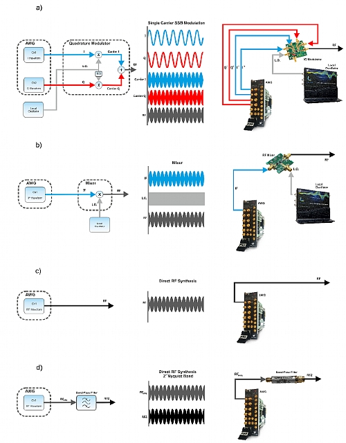
Figure 2.1 AWG Vector Signal Generation Methodologies
I/Q modulation is very sensitive to any inaccuracy affecting the I and Q components and the orthogonal fc carriers applied to them. A good way to visualize the influence of these inaccuracies is by applying two FM sinewaves with a 90O phase difference. The figure below depicts that in a perfect situation, the modulated I and Q components are added together in one of the fc±fm sidebands and are cancelled in the other (top left). If amplitudes of the I and Q components are not the same, cancellation is not perfect, and the Quadrature Imbalance impairment shows up (bottom left). If relative phase for carriers are not accurate, an unwanted residual sinewave shows-up resulting in the Quadrature Error impairment (top right). Finally, if some DC component is added to any of the modulating sinewaves or carriers, an unwanted residual carrier will appear (bottom right). This impairment is known as Carrier Leakage. In the real world there may be some other linear and non-linear impairments with similar effects. As any complex-modulated signal can be seen as the addition of infinite sinusoids, these impairments result in the signal interfering itself and reducing the signal-to-noise ratio. Identifying and measuring these impairments independently is necessary to apply corrections to reduce them. This can be quite difficult and time-consuming to do. Numerical quadrature modulation does not suffer this problem as all the components behave ideally.
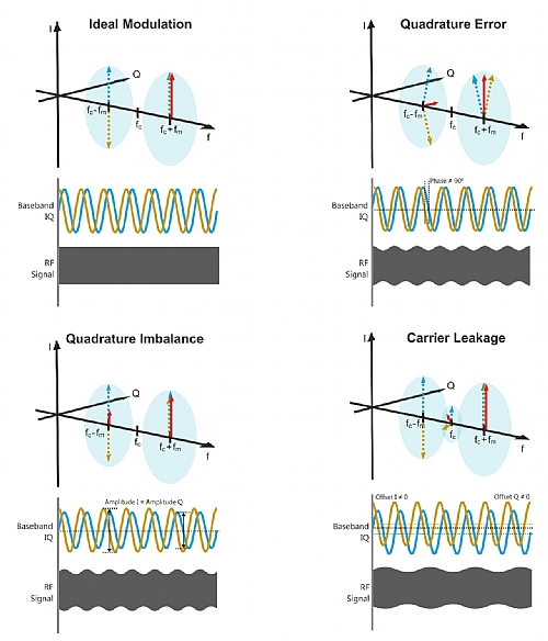
Figure 2.2 Ideal Modulation and Various Impairments
Any AWG can generate complex modulated IF/RF signals by just calculating the complete, modulated waveform and transferring it to the waveform memory. The sampling rate for the calculated and the generated waveforms will be the same and it is related to the carrier frequency.
The figure below depicts a different approach that is implementing in hardware a DUC (Digital Up-Converter) (here, a block diagram of the DUC implemented for each DAC in the Proteus series). The most important advantage consists in the fact that the waveform memory will store complex sample pairs (I/Q) that will be demultiplexed internally to two different multipliers where they will be combined with two orthogonal carriers generated by two NCOs set at the same frequency (fc) and 90O differential phase. As the I and Q waveforms are not related with the carrier frequency, these waveforms can be sampled at a sampling rate enough for the modulation bandwidth (basically sample rate >= modulation bandwidth). In order to match output sampling rate and the baseband waveforms sampling rate, an additional interpolation block must be added. In real DACs, interpolating factors are limited to a set of integer values so there is an integer relationship between the input and the output sampling rates. This scheme has several advantages as memory and calculation time is saved and the fc can be changed without having to recalculate the waveform, even on the fly.
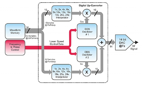
Figure 2.3 Proteus Block Diagram of the DUC Implemented for Each DAC
The figure below depicts that the capture of RF signals using a digitizer is quite symmetrical to the way AWG generate them with the signal flow going in the opposite direction. An external IQ demodulator can feed two digitizer channels (a), or a mixer can generate an IF signal at a lower frequency that can be digitized using one channel (b). If sampling rate and analog BW are enough, the RF signal can be directly captured in the first Nyquist zone of the digitizer (c) or in a higher order Nyquist band by under-sampling (d). In this case a BPF must be used to remove any signal located in the other Nyquist bands, if any.
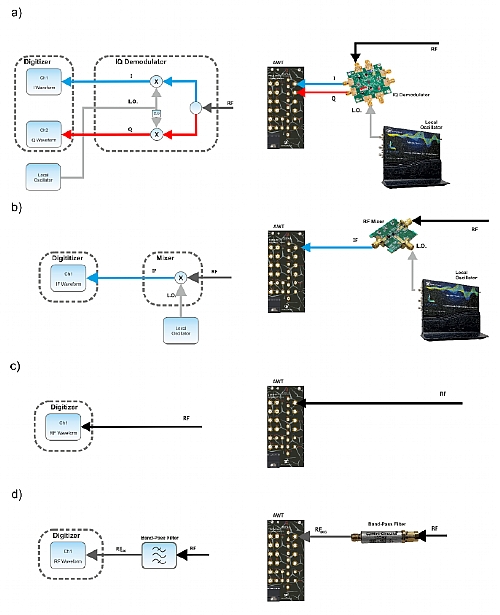
Figure 2.4 Capture of RF Signals Using a Digitizer
Eventually, if the sampling rate of the AWG is high enough, a modulated RF carrier can be generated directly (Figure 2.1, c). In this case, the requirements for the sampling rate will be even higher as the final carrier frequency will be higher than any IF frequency. It is true that ENoB (Effective Number of Bits) decrease as sampling rate grows, but the resulting quantization noise is spread over a wider BW, so the noise power density does not grow that much. When sampling rate is not enough for the target carrier frequency, an image located in a higher order Nyquist band can be used instead if the analog BW allows (Figure 2.1, d). AWGs such as the SE5082 incorporate DAC modes (RF mode) designed to minimize the amplitude of the image in the first Nyquist Band and emphasize the images in the second and third Nyquist band. Typically, a BPF is connected at the output to get rid of the undesired images. The main advantage of this RF generation scheme is the simplicity of it as no external devices (i.e. mixers, modulators, or L.O. sources) are necessary.
IF/RF direct generation requires higher sampling rates but less channels than baseband generation. It also requires higher sampling rates, and a higher sampling rate results in a larger waveform memory if the same time window must be generated. In order to ease those requirements, some RF-oriented AWGs, such as the Proteus family, incorporate an internal real-time I/Q modulator or DUC (Digital Up-Converter) (Figure 2.3). The beauty of real-time I/Q modulation is that it is associated to an ideal interpolation block so the I/Q sample pairs (now stored together and interleaved in the same waveform memory) are fed to the DAC block at a much lower sampling rate, defined by the modulation BW, so waveform memory and calculation and transfer time is greatly reduced. Additionally, the carrier frequency can be changed without modifying the I/Q waveform, just by setting the NCOs to the new frequency.
The same basic architectures can be also applied to the acquisition of modulated RF signals using DSOs or digitizers (Figure 2.4). In particular, it is possible to directly capture an RF signal even beyond the first Nyquist band by under-sampling the input signal if the analog BW of the digitizer is high enough. In order to do so, the center of the useful Nyquist band must be aligned with the RF signal to be captured by setting the appropriate sampling rate (Figure 2.5, a). Doing so, the waveform will show up as an image in the first Nyquist band. Depending on the Nyquist band being used, the spectrum of the image signal in the first Nyquist band will be reversed. Any other signal in any other Nyquist band will interfere with the target signal, so it may be necessary to apply a BPF to the input. The waveform can then be stored in the acquisition memory and further processed afterwards. Sampling rate and memory requirements for the acquisition are linked to the ADC sampling rate. However, the digitizer waveform could be processed in real-time through a DDC (Digital Down-Converter), an I/Q demodulator, figure 12b) to I/Q baseband and decimated so the final sampling rate is equal or higher than the modulation BW and not set by the carrier frequency. This operation also results in a “processing gain” (in effective bits) caused by the original oversampling respect to the one after decimation. A lower sampling rate results in lower waveform memory requirements and, even more importantly, faster waveform processing, a critical need for closed loop control.
The AWG section of the Proteus family is a good example of a direct-to-RF arbitrary waveform generation. All the Proteus models share the same DAC platform. However, the 1.25GSa/s and 2.5GSa/s maximum sample rate models can work in the 16-bit mode only. The 9GSa/s mode can still work in the 16-bit mode up to 2.5GSa/s but an additional working mode extend the sampling rate in direct conversion to 9GSa/s with 8-bit samples. Additionally, the 16-bit mode combined with the built-in real-time interpolation and DUC, allows for the generation of RF waveforms up to 7.5GHz (first and second Nyquist band) with high-resolution waveforms and excellent dynamic range and modulation bandwidth (>2GHz). Higher modulation bandwidths (>4GHz) can be still reached through the 8-bit mode. One of output stage options is especially designed for higher performance RF and mW signal generation. It removes any amplifier from the signal path, so linearity and bandwidth are improved. Additionally, it is AC-coupled as many RF devices are very sensitive to any remaining DC offset. SFDR (Spurious-Free Dynamic Range) specification offered by this option is excellent and can be >80dB over the full usable BW and even >90dB in the 1-2GHz range.
The Proteus DUC is a very flexible and powerful one. The DUC can be combined with the built-in interpolator so the waveform sampling rate can be adapted to the modulation BW rather than the carrier frequency. Interpolation factors supported are 2X, 4X, 6X, 8X, 10X, 12X, 16X, 18X, 20X, and 24X (Figure 2.6, a). Such flexible choice allows for an optimal effective sampling rate selection and the corresponding waveform memory savings. Interpolation, to be useful, must be combined with the application of a high-quality interpolation low-pass filter. The digital interpolation filters applied for every interpolation factor are excellent and show a 0.01dB ripple in the passband BW (0.4 X input waveform sampling rate) and a stopband attenuation higher than 90dB (Figure 2.6,b). NCOs are a very basic component of any DUC. Two NCOs working as a single quadrature oscillator are required for IQ modulation. The Proteus internal architecture allows for independent control of both frequency and phase for each 48-bit NCO in the IQ modulator. For regular IQ modulation, both NCOs share the same frequency while phase difference is set to 90o. Relative phase control is also possible between multiple channels in the same or multiple Proteus modules. This characteristic is paramount in any multiple RF channel generation application where carrier coherence is required. Phase-array radar, MIMO, and Qubit control are just some of these application areas.
The Proteus AWT digitizer section can work in two modes. In the basic mode all the channels can work up to 2.7GSa/s with 12 bits of vertical resolution. In the fast mode, every two channels can be combined to offer 5.4GSa/s sampling rate. Besides being usable as a regular digitizer from DC up to SR/2, it has been designed to be used as an IF/RF/mW acquisition system. Analog BW is excellent (>8GHz), and it can acquire bandwidth-limited signals (i.e. modulated carriers) in the second, third, and even the fourth Nyquist band. Supported modulation BW can reach > 1.3GHz for the basic mode and over 2.5GHz for the fast mode. The Proteus architecture also allows the implementation of additional waveform real-time processing implemented as standard blocks in the embedded FPGA. One of the blocks implemented is a DDC (or an I/Q demodulator). The DDC results in a stream of complex, baseband IQ samples that can be filtered and decimated based in the application needs. The sampling rate reduction results in an easier later processing and acquisition memory savings. The software trigger system can also trigger the acquisition based in the RF instantaneous power or RF pulse duration. Acquisitions can incorporate pre-trigger information and multiple frame time-stamped acquisitions with extremely low dead-time are possible. Data reduction can help in speeding up signal processing and even identification.
Figure below. In order to store and process an RF signal captured by a digitizer, it must be properly digitized. Waveforms captured by any ADC can be modelled as waveforms located in the first Nyquist band (DC-SR/2). When the analog BW of the ADC and the aperture time of the S/H circuit is small, any waveform fitting completely in any of the Nyquist band below the analog BW of the digitizer can be successfully captured as it was down-converted (a). Depending on the Nyquist band being used, the captured waveform will be reversed in the frequency domain. Any BW-limited signal in the first Nyquist band can be down-converted to complex baseband components (IQ) by applying a DDC (Digital Down Converter). Again, the DDC block diagram is very similar to a DUC with the signals flowing in the opposite direction. Sampling rate can be reduced (by decimation) according to the modulation bandwidth of the signal. Reducing the sampling rate improves waveform storage requirements and signal processing. The below figure shows how a 6.25GHz signal can be captured by a 5GSa/s digitizer with more than 2GHz Analysis Bandwidth.
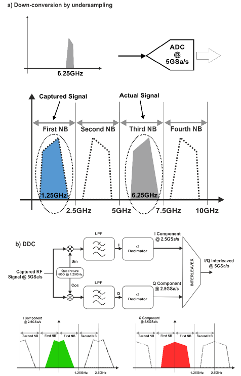
Figure 2.5 Capture of RF Signals Using the Proteus Digitizer
The figure below depicts the DUC implemented in the Proteus DACs that is extremely powerful and flexible. One of the advantages of the architecture is that the initial phase for all of the NCOs in the different DACs can be set independent and coherently so the relative phase of all the carriers can be controlled. The FPGA can incorporate standard blocks for real and complex signal real-time corrections so modulated signals can be corrected for any carrier frequency (a). A critical component of any DUC is the interpolator (b). In the Proteus DACs the interpolator is composed by a zero-padding block and an interpolation/antialiasing filter. This filter is different for each interpolation factor. They are designed in such a way that they show near-perfect flatness for frequencies up to 0.4xfbb (sampling rate for the baseband components) and a >90 dB rejection for frequencies > fbb/2.

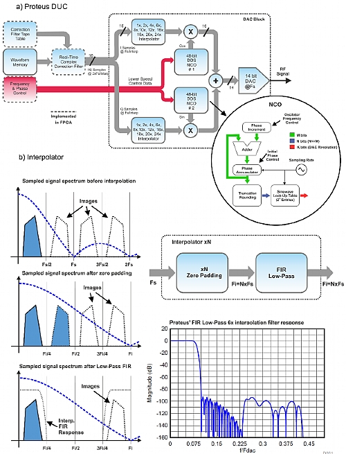
Figure 2.6 DUC Implementation in Proteus
3 High-Precision Waveform Generation and Acquisition
Real-World high-speed arbitrary waveform generators and digitizers cannot implement a perfect flat frequency response with a linear phase (fixed delay) behavior over the full bandwidth. Even more, it is virtually impossible to reproduce exactly the same response for all the instruments and, even, for all the different channels in the same device. Some applications can cope easily with such limitations. Others, such as qubit control or wireless test, cannot. The solutions to this problem are calibration and corrections. Additionally, the frequency response of the generator is just one of the factors influencing the overall response. It is also important to characterize all the signal chain including cables, connectors, amplifiers, filters, attenuators, fixturing, and any other item that can influence the response. In some cases, frequency response data may be already available or can be obtained separately (i.e. as a S-parameter file in a standard format such as the Touchstone© format). For some others, it is better to characterize the system at once.
Knowing the frequency response (magnitude and phase) of any component in a test or control system is the first step. The concept of characterizing the linear frequency response of an AWG is quite simple. A known signal covering the band of interest is generated and the actual output after the signal chain is then characterized (Figure 3.1). The problem is solved after finding the frequency response that gives a better approach to the output waveform for the input waveform. In AWGs, generating signals suitable for calibration is relatively easy as these signals are defined as mathematically ideal waveforms. There are many candidate signals suitable for calibration. Some of the most useful signals consist in different multi-tone arrangements. Multi-tone signals are typically composed by equally spaced tones. Phase for each tone can be random or accurately controlled to improve the overall power. The higher the power, the better sensitivity, dynamic range, and noise resilience of the calibration performed. The “parabolic” phase distribution provides a near-optimal crest factor and a very good pdf (probability density function) over the whole dynamic range of the AWG’ DAC (Figure 3.2). Users can control easily the frequency resolution by controlling the spacing of the tones. Good quality calibration requires the disconnection between the quantization noise and the frequency response. Calibration signals are calculated in a way that an integer multiple of cycles fit in the time window resulting from the selected waveform length and sampling rate so it can be looped seamlessly without any wrap-around artifact. The minimum time widow must be, then, equivalent to one cycle of the tone of the minimum frequency to be characterized or the spacing between carriers. In most realistic calibration scenarios, both frequencies (minimum and spacing) are the same. The problem with this setup is that quantization noise and any non-linear distortion will repeat at the same frequency of the waveform so all the noise and distortion power will go to exactly the same locations of the calibration tones in a coherent way as the phase relationship will be constant and, as a consequence, both the amplitude and phase of the tones will be changed and the accuracy of the calibration compromised (Figure 3.3, a). In order to avoid that problem, the best way is fitting multiple repetitions of the original time window making sure they do not repeat exactly in the same way for each occurrence. This can be accomplished in two ways. The first one is just appending multiple copies of the same basic waveform and then apply dithering (just a very small noise addition to make sure that quantization noise does not repeat for every occurrence of the basic waveform). The second way to obtain a similar or better result is selecting an overall waveform length and an integer number of repetitions so every occurrence of the basic waveform requires a non-integer number of samples although the overall, combined waveform does (Figure 3.3, b). In both cases, noise will be distributed at multiples of the overall repetition frequency, much lower than the tone spacing, and just a fraction of it will fall in harmonics located at the same frequency calibration tones do. As the overall noise power is the same, the average power for the interfering harmonics is reduced in the same proportion. Repeating the same basic calibration signal 10 times will reduce the interfering noise power by 10dB.
The figure below depicts that signal source calibration is a quite straight forward process. AWGs are ideal as calibration waveforms are mathematically defined. Maximally flat response oscilloscopes are also ideal for this calibration process as any >10GHz scope bandwidth from any major manufacturer shows an extremely flat frequency response (internally corrected). Once the AWG + cabling + fixturing response is acquired, a correction filter can be calculated. This correction filter can be applied by pre-processing of the waveform before being transferred to the AWG or applied in real-time using an internal FIR implemented in the AWG’s DAC, whenever is possible as it happens in the Proteus AWG.
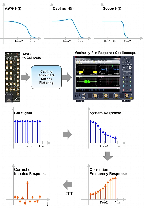
Figure 3.1 Signal Source Calibration
Figure below: A very useful signal for AWG and digitizer calibration is the multi-tone signal. It is made of multiple equally spaced, equal amplitude tones. The problem of such signals is their tendency to use unevenly the available DAC (or ADC) dynamic range and show a poor PAPR (Peak to Average Power Ratio). Both issues cause inaccurate, noisy results and boost the influence of any non-linear behavior in the calibration results. Fortunately, there are specially designed phase distributions for the tones that result in very low PAPR values and with a much more consistent distribution of the signal over the full converter dynamic range. Here, the parabolic phase distribution behavior is shown. PAPR is just 2.6dB as it is independent of the number of tones (constant phase distribution shows a 20dB PAPR while pure random phase distribution results in PAPR in the range of 7 to 12dB, both for 100 tones but this value grows with the number of carriers).
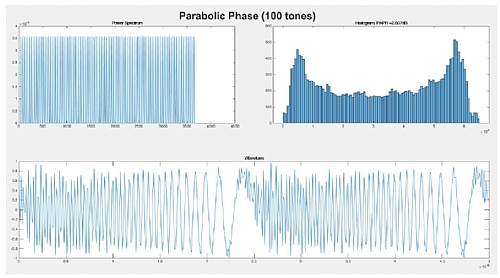
Figure 3.2 Multi-Tone Calibration Signal
Selecting the frequency resolution of the frequency response characterization is not a trivial task. The overall frequency response for a wideband system is a combination of effects that can be better described by either “lumped-element” or “distributed-element” models. While lumped-element frequency responses can be properly characterized by a rather coarse frequency resolution, distributed-element sections may require a much finer frequency resolution. A good example of such distributed-element behavior are cables and fixtures where reflections occur due to impedance-mismatches. The only way to correct for these reflections is by using long correction filters and those can only be obtained from high-resolution frequency responses. In other words, the length of the impulse response of any correction filter must be at least as long as the length of the impulse response to be corrected.
Generating the right golden calibration signal is just the first step for a successful calibration. Any calibration procedure requires a reference to be compared to as accurate as possible. A very important issue with AWG calibration is the need to characterize both amplitude and phase. This means that traditional spectrum analyzers cannot be used for proper calibration as they only provide magnitude information. Fortunately, modern high-bandwidth oscilloscopes come to the rescue. In the past, frequency response for oscilloscopes was purposely designed to be as close to gaussian as possible as this kind of response did not show any overshoot or ringing in its step response in the time-domain. Implementing such response in a high bandwidth real-time digital oscilloscope (RT-DSO) results in extremely high sampling rates to meet the Nyquist sampling criteria. A typical midrange 8GHz BW (20GSa/s) scope from a major manufacturer offers a +/- 1dB flatness and a 7o maximum deviation from a perfect linear phase response from DC up to 7.5GHz. Other higher-end products show even better amplitude flatness (0.5dB) and phase linearity responses over even higher bandwidths. This excellent flatness performance is obtained through internal corrections according to careful calibration in the factory using very well defined and characterized ultra-wideband pulse generation devices. In a typical calibration setup, the AWG to be calibrated along with all the signal transmission chains are connected to the oscilloscope either directly to the input or through a compatible high-impedance, high-bandwidth probe. Multiple AWG channels could be connected to different channels in the oscilloscope so simultaneous calibration of multiple channels could be performed. However, a better matched response among AWG channels will be obtained by sequentially performing the calibration procedure using the same scope channel. The process starts with the capture the time-domain waveform with the scope and performing an FFT with a convenient time-domain window (i.e. flattop). Then, reading the magnitude and phase values at the frequencies of the calibration tones and comparing those with known values for the ideal signal, will produce a series of magnitude/phase vs. frequency values. Scope must be triggered using the same sync output from the AWG regardless of the channel being calibrated. Doing these, any skew (differential delay) between channels will be embedded in the phase response so correction filters applied to the waveforms will automatically align all the signals in the time-domain (Figure 3.1).
The figure below depicts that the effects of quantization noise over the multi-tone calibration signal may be not negligible. In a) the calibration signal is generated by looping the basic multi-tone cycle. As the same samples repeat for every loop, so does the quantization noise. As a result, all the noise power goes to the exact location of the tones, interfering with them and causing amplitude and phase errors. In b) waveform length has been selected to accommodate three repetitions of the same basic waveform. However, if the waveform length is selected so it is not a multiple of three, the three occurrences of the basic signal will not be the same as the sampling times will fall in slightly different instants. The spectrum of the signal will still be the one corresponding to the original tones. However, quantization noise will be repeated with 1/3rd of the period so its spectrum will consists in three time the number of lines while the overall power will be the same, so the interfering components of the noise will have less power and accuracy for the calibration tones will improve. In order to get the best results, the number of repetitions and the waveform length do not have to share a divider other than 1. A good way to accomplish this is by selecting a prime number for the number of repetition and making sure the waveform length is not a multiple of it.
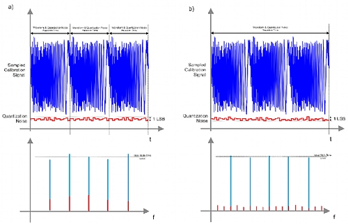
Figure 3.3 Effects of Quantization Noise Over the Multi-Tone Calibration Signal
The methodology described above works very well for wideband signals. However, for narrowband RF signals, the accuracy of the correction in terms of frequency resolution to reach a good modulation accuracy must be improved while the frequency response out of the band occupied by the signal is irrelevant. In this situation, an alternative calibration methodology based in adaptive equalization techniques can be used. The calibration signal may be any modulated carrier with a known modulation and a sufficient signaling speed to cover the full targeted band. The signal can be then captured by a scope or a VSA (Vector Signal Analyzer). A demodulation software executing an adaptive equalizer filter algorithm will obtain directly the complex correction baseband filter (Figure 3.4, top). This filter could be applied to the complex signal modulating the carrier for any modulation (the linear model is the same for every modulation).
The frequency response obtained during the calibration process can be used to calculate a correction filter using different time-domain or frequency-domain techniques. These filters should be applied to waveforms during the calculation process before being downloaded to the target AWG, or through a real-time FIR filter implemented in the target channel if the AWG hardware allows for it (Figure 3.4, bottom). The advantage of using real-time filters is that the waveform can be calculated independently of the target instrument and channel. Additionally, any change in the signal path modifying the frequency response only requires recalculating the filter taps once and not all the waveforms. For AWG incorporating DUC with IQ modulators, real-time corrections can be applied to the I/Q complex waveform at a much lower sampling rate or to the modulated waveform at the final sampling rate. Applying the correction to the complex I/Q baseband signal is a much better approach as the real-time DSP is performed at a lower speed and the number of taps required will be much reduced for the same level of correction accuracy (Figure 3.4).
Calibration should be performed for all the different DAC and output modes available in the AWG and at different sampling rates and amplitude levels. The overall frequency response of any DAC depends on the sampling rate as even ideal DACs show a sinc(f) response with a zero at the sampling rate (zeroth-order, or ZOH, response). A proper characterization of the frequency response of the system must subtract the influence of the ZOH at the calibration sampling rate and then apply the one corresponding to the actual sampling rate selected for the waveform before calculating the correction filter. However, some DACs incorporate an internal digital 1/sinc(f) digital filter so users must apply corrections based in the frequency response without having to correct for the ZOH response corresponding to the sample rate used in the calibration. Calibration procedures can be extended beyond the first Nyquist band. The images of the calibration signals at higher order bands can be used to calibrate the response of the generator for the generation of RF and mW modulated signals at those frequencies.
Figure below: VSAs (or DSO with VSA software) can be used to efficiently calibrate the response of an AWG (and any additional component) by directly generating a digitally modulated carrier (i.e. QPSK) with a high enough baud rate to cover all the band of interest. All the linear impairments in the system will influence the modulation quality in terms of the received constellation diagram and measured EVM. Advanced BSA software can identify the system response in order to apply aa adaptive equalizer correction (a complex FIR) to compensate for linear distortions. The frequency response (or the equalizer coefficients themselves) can be extracted so they can be applied to the signal being generated by the AWG. The corrected waveform will have a much higher accuracy than the original one and the usage of the equalizer will not improve any measurement in the VSA. Here, a 1.5GBaud QPSK signal is used to characterize over 1.5GHz of bandwidth around the carrier frequency. The overall EVM measurement for the uncorrected signal is around 5% while the EVM for the corrected signal is around 1%. In the Proteus platform, complex corrections can be applied in real-time to the baseband complex signal using a correction filter implemented in the FPGA. This methodology provides very good results for bandwidth-limited signals as frequency resolution may be very high.
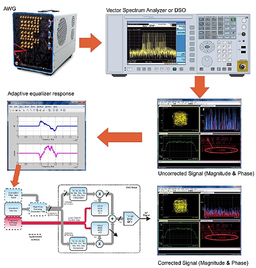
Figure 3.4 VSA Used to Calibrate AWG Response
Instrument calibration and waveform correction is part of the Proteus series solution. The WDS software (Figure 3.5) incorporates a tool to calibrate AWGs and associated components and calculate and apply correction filters for any Nyquist band. Frequency response for each channel is characterized in the factory and the corresponding correction factors can be read using SCPI commands and supplied in a CSV file. The WDS correction tool can combine the factory-supplied frequency response for the instrument with any combination of frequency response or correction factors from different sources and formats such as the Touchstone© S-parameter file format produced by almost any frequency or time domain VNA, or adaptive equalizer responses from VSAs. Once the frequency response is obtained, users can obtain a correction filter and analyze the corrected response. Users can specify the complexity (number of taps) of the filter and validate the accuracy of the correction within the same tool. Once the correction filter is designed, it can be applied to any real or complex (I/Q) waveform created within or imported by the WDS application. Corrected waveforms can be then downloaded to the target instrument and channel. The Proteus DAC incorporates a x/Sin(x) filter to compensate for the ZOH response. This means that there is no need to subtract the ZOH response from the frequency response data and add it again (at the same or a different sampling rate) before calculating the correction filter.
The figure below depicts how the WDS (Wave Design Studio) software is used as the SFP (Software Front Panel) of Proteus (or any other Tabor AWG). It can be also used (online and offline) as a powerful waveform edition and import tool (i.e. from MATLAB © or any DSO). Here, a Gaussian-envelope RF pulse have been designed using the formula editor. Time aligned marker (digital outputs) content has been also defined. The WDS tool can be also used to define complex sequences and triggering schemes. The same environment can also set up the digitizer and visualize any captured waveform as an oscilloscope. WDS can be extended by adding functional (Instrument calibration, correction) and application oriented (i.e. Radar or multi-tone) add-ons.
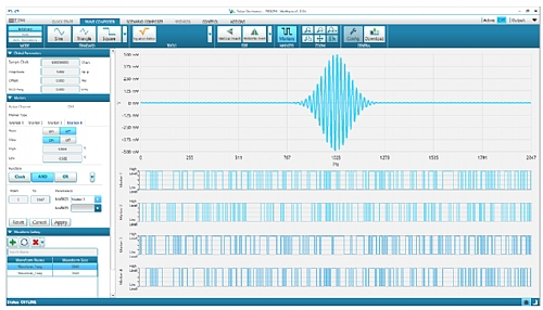
Figure 3.5 WDS Software Usage as a Software Front Panel for Proteus
The Proteus architecture allows for a different correction implementation, also supported by the WDS correction tool. It consists in implementing corrections through the application of a real-time FIR filter implemented in the FPGA block. Corrections can be applied to the waveform before being converted to analog (real-only taps), or to IQ waveform pair before being fed to the DUC (complex taps). The second choice is better for IQ modulated signals, especially for relatively narrowband signals as it requires much less taps to reach the same level of correction accuracy. FIR blocks can be activated and set up using SCPI commands or directly from the WDS environment (Figure 3.6, a & b).
The figure below depicts how corrections can be applied in real-time in the Proteus platform thanks to the DSP functionality implemented in the built-in FPGA. It can be applied to the AWG channels in both the direct (a) and the up-converted (b) modes an also in the digitizer channels in both the direct (c) and the down-converted (d) modes. The digitizer channels and any cabling and device attached to them can be easily calibrated once the AWG channels are calibrated and corrected. Once characterized, a correction filter can be calculated and applied.
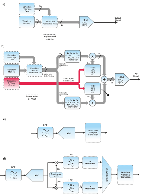
Figure 3.6 Real-time Signal Correction Block-Diagram
Calibration is another capability of the WDS application. Fully automated calibration is possible after defining the desired frequency range, operating mode and sampling rate. The calibration software supports a variety of high-BW, maximally flat frequency response oscilloscopes from manufacturers such as Keysight, Tektronix, LeCroy or R&S. The WDS also supports the generation of QPSK signals with known modulation characteristics (baseband filter, roll-off factor) at any symbol rate and carrier frequency so the right adaptive equalizer or channel model can be obtained by any VSA or scope equipped with VSA software.
Once the AWG section of the Proteus AWT have been properly calibrated, it can be used as the source of calibration signals for the Digitizer section. The WDS correction application also supports digitizer calibration and correction of the acquired waveforms for any of the Nyquist bands up to >7GHz. Again, the Proteus architecture allows for the implementation of the correction filters in real-time right after analog-to-digital conversion (real-only taps) or to the complex waveform (I/Q) after applying the DDC block, including decimation. This is also important as the digital trigger system can work directly over the corrected data so trigger events will be detected more accurately and consistently (Figure 3.6, c & d).
4 Real-Time Control of Operating Quantum Computing Systems
4.1 Closing the Loop
The AWT concept implemented by the Proteus platform is not just a convenient combination of an AWG and a digitizer in a single device, it is a full-fledged closed-loop processing and control solution (Figure 4.1, a). Each basic Proteus cell (4-Channel AWG @ 2.5GSa/s or 2-Channel AWG @ 9GSa/s combined with 2 Digitizer Channels @ 2.7GSa/s or 1 channel @ 5.4GSa/s and up to eight 1.25Gbps marker outputs and 2 GPIOs) incorporates a powerful FPGA from Xilinx, the UltraScale KU-060 model, tightly connected to all the analog and digital input/output blocks (Figure 1.10). The current implementation allows for the future incorporation of even more powerful and faster FPGAs. The current FPGA supports more than 700K logical cells, 2,700 DSP slices and 32 transceivers@ 16.3Gbps. The FPGA is also used by the standard Proteus functionality. The FPGA can be sued in closed-loop application in several ways (Figure 4.1, b).
The figure below depicts how Proteus units can be used for closed loop control of complex systems such as quantum computers. Loop can be closed internally through the built-in FPGA or externally through other Proteus units (or any other compatible hardware) through the high-speed (60Gbps) PCIe Gen. 3 backplane in a PXI chassis (a). The internal FPGA offers a huge unused processing capacity to implement any desired functionality in different ways (b). The standard Proteus functionality supports a “Decision Block” capable of controlling the AWG sequencer according to user-defined events coming form the analog, digital or trigger inputs. Optionally, users can obtain application-specific sets of processing blocks than can be defined and connected using SCPI commands without any need to develop IP for the FPGA. Finally, users can develop their own IP or use existing one (i.e. ARTIQ). For those users, the Proteus Shell is made available to designers so all the access to the internal HW and resources (PCIe bus, DRAM) is already designed.
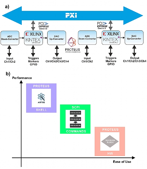
Figure 4.1 Proteus Used for Closed Loop Control of Complex Systems
The first usage model does not require the implementation of application specific processing blocks, just the standard functionality. The digitizer alone can generate events through the so called “decision block”. The events generated by this bock can be used by the most powerful AWG sequencer available in the market combined with timers, external trigger events, etc. It supports conditional branching so waveforms to be outputted can be selected depending on external conditions. Dynamic sequencing (where the segment to be generated is selected by a digital parallel input port) is also possible in Proteus. The total or partial implementation of some waveform segments in the FPGA’ RAM (instead the massive DDR4 memory that can be only accessed in big blocks) greatly reduces some of the problems in high-speed AWGs with long waveform memory: trigger latency and trigger jitter.
Standard or optional application-oriented processing blocks. Multiple packages of hardware functionality will be offered. Using those, user can wire up different already defined processing blocks defined by Tabor Electronics in order to solve a specific processing chain/closed loop functionality. Instead of having to design this functionality using an eternal FPGA design tool, users can just use SCPI commands to set up the processing elements and stablish the signal flow. Some of the processing blocks (i.e. the DDC or the FIR filters) have been previously described in this paper. Some other are tightly connected to specific application areas such as quantum computing, wireless network, or Radar.
“Shell” based solutions where users design all the functionality using any available FPGA design tool while Tabor Electronics supply the IP “Shell” that provides easy access to all the Proteus HW without having to deal with all the critical timing and functional requirements related with the high-speed signals generated and acquired by the Proteus platform and the integration with the DDR4 massive RAM memory and the access to 3rd Generation 8x PCIe bus (50Gbps communication speed). This approach hides all the complexity of the Proteus platform to users while giving full freedom to designers to create their own solution. This is an ideal solution for very complex closed-loop environments and even for the prototyping of proprietary closed-loop systems.
4.2 Modularity and Scalability
Operational quantum computing systems and other applications (i.e. massive MIMO, phase-array RADAR) may require tens of analog inputs and outputs combined with multiple digital inputs and outputs. A typical qubit may require two analog channels to control the state of the qubit and one channel to read its state at very specific, tightly controlled moments in time. Some digital signals may be also necessary as well. Just one Proteus PXI module could then control up to two qubits simultaneously. A single 21 slot PXIe mainframe can hold up to 10 AWG Proteus cards so 40 AWG channels can be supported in it (Figure 4.2). Embedded PXI controllers or external computers connected through very high-speed optical interfaces to the PCIe bus could even implement the closed-loop processing and control. The PCIe implementation in the Proteus platform, allows for sustained transfers at 50Gbps (or >6GSa/s @ 8bit resolution) from/to any external device. However, when real-time processing and low latency closed-loop control is necessary over more than a few channels, the external controller is not the answer. There are too main reasons for it. First, the PCIe bus, even in its highest performance implantations will become a bottleneck as it should be shared by multiple channels from multiple modules. Secondly, because any external computer will run out of processing power for a relatively small number of channels. There are other issues, such as the latency time (very important in close-loop control) or the deterministic behavior of the processing system. Th Proteus solution, where an FPGA is incorporated to any basic Proteus block, avoids transferring unnecessary information through the PCIe backplane while the processing power grows with the number of channels in a predictable, proportional manner. User can implement signal and data processing using a general-purpose processor implemented in the FPGA (i.e. an ARM processor) or using application-specific hardware processing or a combination of both. The traffic in the PCIe bus can be reduced to configuration, supervisory and monitoring data to/from the control computer or for information shared of transmitted between modules.
The channel density and the fact the internal processing power escalates with the number of channels make the Proteus platform ideal for applications where many input and output channels are required and may need to grow in the future. In the below figure, two Tabor PX21100 PXIe optical chassis hold a total of 17 Proteus modules of different models, both AWG and AWT. The chassis in the top includes 7 AWT modules (3 slots each) with 28 AWG channels, 14 Digitizer channels, and 56 digital (marker) outputs. The chassis in the bottom holds 9 AWG modules and 1 AWT module with up to 40 AWG channels, 2 digitizer channels, and 80 digital outputs. Multiple chassis can be synchronized to work as a single unit. The optical PCIe extender supported by this chassis allows for a 100Gbps connection to any controller so there is no need to integrate an embedded PXI controller to access the PCIe backplane at full speed.
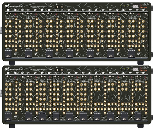
Figure 4.2 Proteus for High Capacity and Scalable Applications