Relevant Documents
 (902KB)
RF and Microwave theory sits on the shoulders of Maxwell, and Hertz with the theoretical development of the connection between electricity and magnetism that started in the early 1800s. Today the use of RF and Microwave radios are ubiquitous, used by everyone every day, but still, the subject remains complex and takes many years to learn.
In this article we will start with the fundamentals of wave propagation, understanding the difference in wave velocities through a vacuum vs cables of different types and lengths. Then we will examine impendence and why it is important – gaining an understanding of impendence matching and transmission lines to ensure maximum power transfer between two devices. The second topic deals with passive frequency translation and how the properties of nonlinear devices - namely diodes, configured as frequency multipliers or frequency summation devices such as mixers - can help modify the signals' frequency. The Frequency Synthes Topic uses many of the same principles as frequency translation and details how to convert a reference frequency to a desired frequency. The next topic covers Modulation and the process of encoding information on to generated frequency – and we will look at AM and Phase Modulation and how they are combined in a vector modulator. We will look at both analog and digital implementations of modulation. Frequency planning is the optimization of the frequency translation path to ensure that intermodulation and harmonic signals do not interfere with the desired spectral purity of the signal we are trying to create. The final topic is Signal Analysis, and many of the fundamentals of synthesis and signal generation equally apply, we will look at different analysis techniques and examine the benefits and trade-offs of each one.
Experiment design considerations for real-time, closed-loop pulse streaming - 50 min workshop
Chapter One – Wave Behavior
A. Velocity
An electromagnetic wave, such as an RF or Microwave signal, propagates through a vacuum at approximately 300 million meters per second (c). However, for a coaxial cable, this can be significantly slower depending on the type of cable. Table 1 shows the specifications of an RG-316 cable.
RG-316 Coaxial Cable
|
Impedance:
|
50Ω
|
|
Capacitance:
|
96pF/m
|
|
Signal Loss:
|
0.79dB/m @ 1000MHz, 1.27dB/m @ 2100MHz
|
|
Velocity of Propagation:
|
69%
|
|
Nominal Delay:
|
5.08ns/m
|
Table 1 – Coaxial Cable Specifications
The speed of signal propagation is defined by the specification - Velocity Factor or Velocity of Propagation and is a function of the dielectric material used in the cable. For example, an RG-316 cable has a Solid Teflon dialectic giving it a velocity factor of 0.69, which means that a wave will propagate through the cable at 69% of the speed of light.
The time it takes for a wave to travel 1 meter can be calculated as

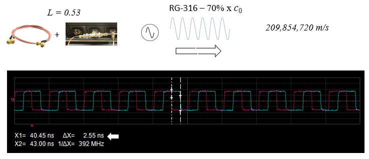
In figure 1 the cable velocity factor is 0.7, and the cable is 0.53 meters in length, so the wave will travel that distance in around 2.5 nanoseconds, as shown on the oscilloscope plot
This time delay can represent a significant phase shift in the signal. If the relative phase of two signals traveling along two cables needs to be minimized, then the cables need to be phase matched, either electrically or (e.g.) by extending the length of one cable until the delay is equal.

Figure 1 – Measuring Wave Propagation through a Coaxial Cable
B. Impedance
When connecting two or more RF or Microwave signals it is important to standardize the connection. RF systems usually define a connectivity impendence of 50Ω. There is nothing special about this value, but matching the impendence is key. In Figure 2a we connect a Tabor two channel Arbitrary Waveform Generator (AWG) to an oscilloscope. Each of the AWG outputs has both a regular output and an inverted output. In diagram 2a we have the non-inverted output connected to CH 2 and CH 3 in parallel as shown by the coaxial T-connector and the inverted output connected directly to channel 4.
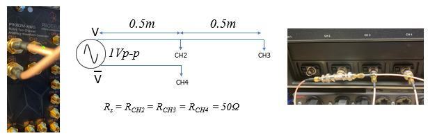
Figure 2a Connecting the Arbitrary Waveform Generator (AWG) to the Oscilloscope
Figure 2b shows the circuits of this setup and the measurement results on an oscilloscope. The direct connection on Channel 4 has a measurement result of 1Vp-p which is what the Arbitrary waveform generator is set to. If there was no source and load impendence, then the voltage would have been 2V. However, our 50Ω standard essentially creates a voltage divider network of the 50Ω source impendence and the 50Ω load impedance, hence we can say when the AWG is set to 1Vp-p we will measure 1Vp-p across our 50Ω load. In the second example, we have the 50Ω impedance of each channel in parallel due to the coaxial T-connector thus creating an overall combined loading impedance of 25 ohms and our measured value as expected is 0.5Vp-p. It is useful in this case to draw out the schematic of the interconnections to understand why the voltage of the signal is not as expected.
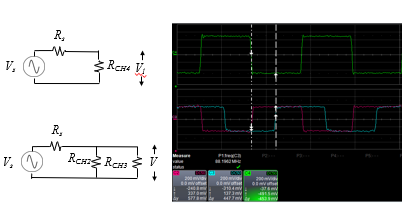

Figure 2b Effects of different load impedances on voltage
C. Transmission Line
A cable acts as if it is made up of groups of inductive and captative elements and as discussed in Section 1A. A wave will propagate through each element with a certain time constant, summing up to the velocity factor over a meter. In Section 1B we stated that if the impedances are all equal, the waves propagate through the system as expected and maximum power is transferred. What if we do not have a matched impedance system? If our load impendence is not matched to the source impedance, then this mismatch will cause the wave to be reflected on itself through the transmission line – Figure 3a., to a point where the addition of the transmit vs reflected waves, creates a summation or superposition that looks like a stationary or a standing wave.


Figure 3a. The capacitive and Inductive Elements of a Transmission Line
This can be demonstrated on an oscilloscope. By using the same connections as in the previous section but changing the input impedance of CH 3 to 1MΩ, we can create an un-matched system. If the AWG is swept from a frequency of 100MHz to 1200MHz with persistence on the oscilloscope set, the superposition of the incident and reflected waves can be visualized as shown in Figure 3b

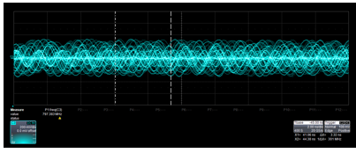
Figure 3b The Superposition of the incident and reflected waves
Figure 3c shows the effects of superposition at different wavelengths. CH2 is 0.5 meters away from the source and CH3 is 1.0 meters away with a high impedance mis-matched load. At 75MHz or a wavelength of 4m the voltage at 1.0 meters is maximized and at 0.5 meters is minimal. At 300MHz or a wavelength of 1.0 meters, the amplitude at each measurement point is equal. At 1200MHz or 0.25m the signal at 1m is completely canceled, while at 0.5m it is at its maximum. The superposition of waves due to mismatched impedance can seriously affect maximum power transfer, and keeping the systems' impedances matched is critical.

Figure 3c. The effects of superposition at different wavelengths
Consider the Transmission Line in Figure 3a. The closer the signal is to DC the inductors conduct more, and the higher the signal frequency the capacitors conduct more or vice versa. This means that there is an associated frequency response of the cable. A spectrum analyzer with a tracking generator can be used to perform a frequency sweep of the cable and verify amplitude attenuation as shown in Figure 3d.

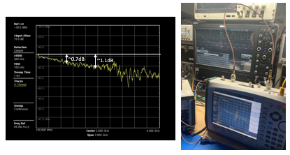
Figure 3d. Frequency Response of the RG-316 coaxial cable
Chapter Two – Frequency Translation
A. Principle of operation
Fundamental frequency translation relies on the properties of nonlinear devices. Consider Figure 4b, a linear device that follows Ohm’s law. If the resistance remains constant a change in voltage across it will proportionally change the current flowing through it. A semiconductor device such as a diode is nonlinear. It does not conduct or conducts very little until the voltage drop across it reaches a certain value, then it begins to conduct. The two red plots show the difference.

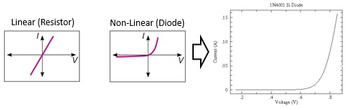
Figure 4a. Linear and non-linear device behavior
There are two types of frequency translation devices – Multipliers and Mixers. Both are based on diodes in a bridge configuration, with filter circuits, and in the case of mixers transformers are used to cancel LO and IF feedthrough frequencies.
An example of a frequency multiplier would be a ‘Doubler’ providing 2x multiplication. It produces output signals at integer multiples of the input signal frequency. For example, if I provide a 1GHz signal the ‘Doubler; will output a 2GHz signal. It will also produce frequency at 3 times, 4 times, 5 times, etc. of the input frequency. However, if the device has been designed well these will be attenuated as shown in Figure 4b.


Figure 4b. A typical frequency multiplier circuit and the measured output of a 2x Multiplier.
A mixer does not multiply the signal but adds and subtracts two signals together. We shall call one frequency the Local Oscillator (LO) and the Other Frequency the Intermediate Frequency (IF). Referring to figure 4c, when an LO is applied the positive swing turns on the green half of the bridge and the negative swing turns on the yellow half, thus only allowing the input frequency current to flow during these on and off times. If the LO frequency is much greater than the IF, which is usually the case, the high frequency switching of the diode circuit produces a time domain envelop of the lower frequency, or effectively adding the LO and the IF.


Figure 4c. A balanced mixer
Using transformers on the input creates a balanced design. A single balanced mixer (which is less common) suppresses either the local oscillator or the signal input at the output, but not both. While a double balanced mixer (the most common) has both its inputs applied to differential circuits, so that neither of the input signals and only the product signal appears at the output, however a double balanced mixer as shown in the diagram requires a higher drive power.
Drive power is important. Too much and you will increase the intermodulation products of the mixer. too little and the mixer will not function correctly as it will be operating in the lower part of the IV curve we showed in Figure 4a.
B. Device Comparisons
There are many manufacturers of mixers and choosing the one that meets the needs of an experiment is important. Table 2 Compares Mixers from Mini-circuits, Analog Devices (ADI), Quantum Microwave, and a digital implementation in the Digital to Analog Converter of a Tabor Arbitrary Waveform Generator.
The Mini circuits mixer is the lowest cost option. It has poor suppression of both the first, second, and third side bands – but requires a relatively low drive power from the LO and has a wide IF bandwidth. The ADI mixer requires the largest drive power, but it effectively suppresses the even products, and the carrier feed through is attenuated by 28dB. The Quantum Microwave mixers are designed for lower noise applications and therefore require a lower LO power, specified at 9dBm - you can see that all the feed throughs and mixer products are well suppressed and that the lower sideband is almost 35db higher than the LO. Finally, the digital implementation has no carrier feed-through, and the unwanted sidebands are well suppressed, however, all the other mixers' operational frequencies are up to 12-15Ghz, the digital implementation is limited to 3.6GHz. In Topic 4 we will examine how to use these devices in multiple Nyquist Zones, plus through effective frequency planning a combination of digital modulation and analog modulation will result in the best signal performance at the required frequency.

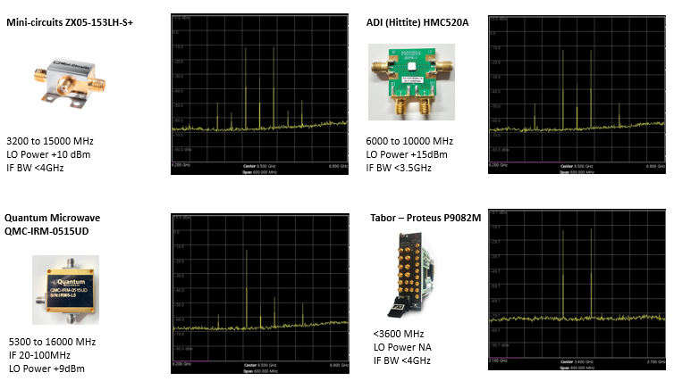
Table 2 – Mixer Comparisons
Chapter Three – Frequency Synthesis
A. Definition
The dictionary’s definition of frequency synthesis is the ability to generate a range of frequencies from a single fixed time-base or oscillator – what is often referred to as the reference.
There are multiple types of synthesis techniques that either fall into the category of direct synthesis – with multiple implementations and both analog and digital designs – or indirect synthesis which is usually an analog implementation.
B. Synthesis Types
Direct Analog Synthesis
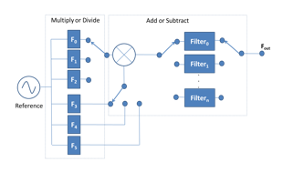

Figure 5a. Direct Analog Synthesis
Direct synthesis is based on analog frequency translation techniques - it is a combination of analog multiplication, mixing, and filtering stages. When higher frequency resolution is required the more complex the combination of stages becomes, however in terms of noise performance, frequency stability, and frequency switching speeds this is the most superior synthesis technique.
Direct Digital Synthesis (DDS)

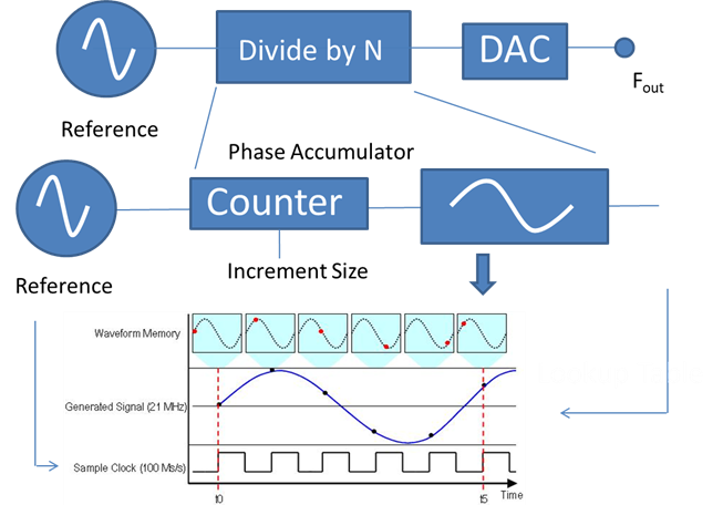
Figure 5b. Direct Digital Synthesis (DDS)
A direct digital implementation stores a waveform in memory, then using and a counter you clock through each memory location at different speeds to produce a relevant frequency. This in effect is a frequency dividing system not multiplication and addition systems like the Direct Analog System. However, the DDS can be used in multiple Nyquist zones to produce higher frequencies. This is explained in Topic Four Section C. RF Digital to Analog Converters and Multiple Nyquist Zone Operation
Indirect Analog Synthesis

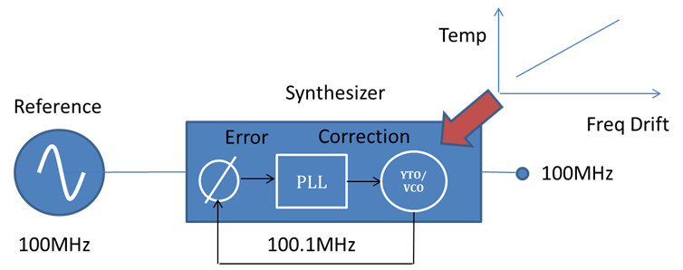
Figure 5c. Direct Digital Synthesis (DDS)
The indirect synthesizer is based on Voltage Controlled Oscillator (VCO) or a YIG tuned Oscillator (TTO) and uses a Phase Locked Loop (PLL) Architecture. The VCO can create a frequency based on a voltage level. The accuracy of that signal is determined by the error between the phases of the reference and the VCO frequency. The PLL compares the phase and produces an error correction voltage.
Arbitrary Waveform Generator
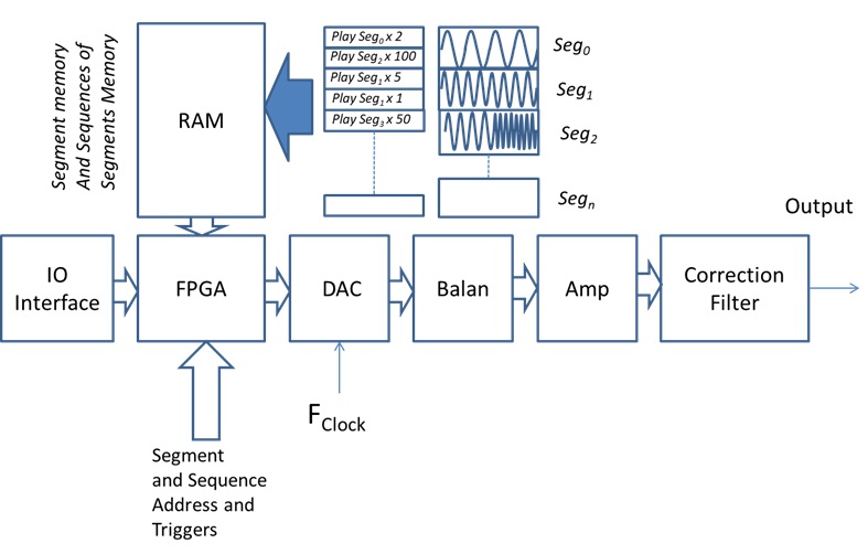

Figure 5d. Arbitrary Waveform Generator (AWG)
An arbitrary waveform generator (AWG) can store multiple waveforms in its memory. These waveforms can be created by specific tools either provided by the manufacturer of the AWG or by using a tool such as MATLAB and Octave. The user can index and play waveform memory combinations. Like with the DDS the highest frequency is a function of the sample clock and waveforms can be generated in various Nyquist Zones.
C. The Reference Oscillator
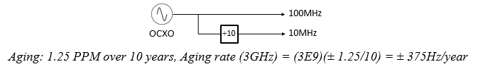
The reference is fundamental as by our definition of synthesis earlier – all our frequencies are derived from it. It also contributes to the quality of the synthesis we wish to perform in our signal generator. Quality can be defined by frequency stability - short term stability, or phase noise. Long term stability is defined by aging or frequency drift. There are multiple references available all with different price points and performance characteristics. Some are built into the signal generator and are based on Oven or Temperature controlled Oscillation Techniques (which are referred to as OCXO, TCXO) and external references that can be derived from a cesium time base (atomic clock) or the GPS system.
Frequency drift is defined by changes in temperature and the aging specification. In this example, you can see when lucid is tuned to 3GHz it drifts 375Hz over a year. This is a factor of 10 improvements over similar signal generators.
If you want to have a number of signal generators phase locked with each other, you would share a single reference between multiple synthesizers or signal generators as shown in 6a.


Figure 6a. Reference Sharing Between Multiple Synthesizers.
In this scenario, we have a single reference being shared between two VCO-PLL synthesizers. If 10MHz is the reference frequency with 0.1° Phase Drift, this will produce a 10° Phase Drift at 1GHz. By changing the reference to 100MHz you receive a ten times improvement. However, this will still cause significant frequency drift problems at higher frequencies. One way to compensate for this is to use a higher reference frequency, preferably in the GHz range. In the example, the Tabor Lucid signal generator is set to 4GHz and with an oscilloscope set to maximum persistence then monitored the two locked sine waves for 15 hours. While not a quantitative measurement, qualitatively it does show there is minimal drift between the two channels over time and temperature
at 4GHz.
Phase Noise

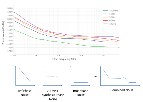
Figure 7a. Phase noise plots
A single side band phase noise measurement is usually used to describe the stability of a synthesizer. In Figure 6a, you can see several effects are in play. The measurements are relative to the carrier and, that carrier would be to the left of the y axis and is often excluded from this type of plot. One phenomenon we observe is the phase noise performance decreases at higher frequency multiples with a rule of thumb of 6dB decrease in performance every time you double the frequency.

Figure 6a can be deciphered in terms of each element of the synthesis technique. Close to the carrier the phase noise is usually related to the reference frequency and has a steep slope, then from around 1kHz to 100MHz you see a plateau based on the noise contribution of the VCO, finally, as you move further away from the carrier broadband noise becomes the dominant factor.
D. Signal Conditioning – Output Section
The final element that determines a signal generator from a synthesizer is the output section. The output section of the signal generator provides us with the required amplitude. It allows for AM modulation, provides gain and attenuation, and ensures that the absolute levels of the generated signal fall within a specified limit. The amplitude range is enabled using attenuators, and in the case of the Tabor Lucid signal generator will allow a signal range of +15dBm to -90dBm to be generated. Up until now, we’ve specifically looked at phase noise, but there are more phenomena that contribute to a degradation in spectral purity. While poor filtering in the synthesis process can cause Harmonics, the active components used to amplify the signal will cause intermodulation, harmonics, and degradation of the broadband noise floor. Intermodulation is caused by two or more carriers constructively interfering with each other and create a frequency related side band. For every dB increase in the carrier, a harmonic will equally increase. For intermodulation, the sidebands increase by a factor of two or three depending on if it is a third order or second order product. The spectrum trace shows the third order harmonics 2f1 - f2 and 2f2 – f1, an example of a second order intermodulation product would be f2-f1, f2+f1. The center plot shows the Harmonic performance of over 60dB’s and finally the third plot represents the broadband noise floor.


Figure 7b. Typical Output Section
Chapter Four – Complex Signals and Modulation
A. IQ Modulation
To be able to transmit information a modulation technique is required. The most popular type of modulator in modern communications systems is an IQ Modulator. It is a combination of an amplitude and phase modulator, thus by mixing different combinations of signals we can create a vector with a certain amplitude and phase. This is represented on a vector diagram. There are two axes, real and imaginary, or I and Q, In-phase and Quadrature components. If the I input has a voltage applied to it and the Q is set to ground, our vector will only have the in-phase component, which would be represented by a horizontal line on the vector diagram. Conversely, if the Q vector has a voltage applied and I is set to ground we would only have a quadrature vector so the vector diagram would show a vertical line. If we apply an equal voltage to both inputs, we can create a vector in between the In-phase Axis or Real Axis and the Quadrature Axis, with a phase shift of 45 degrees. By changing the amplitude and phase difference of each input we can create a multitude of different vectors. In the QPSK modulation example, we apply symbols to each vector point 00, then a shift of pi/2 from there would be 01, a further shift 10, and the final rotation 11.


Figure 8a. IQ Modulator
In many cases an analog IQ modulator requires calibrating. The phase and amplitude need balancing, so we have the correct in-phase and quadrature outputs and minimal carrier feed though. Figure 8b shows two in phase 200MHz tones generated by two channels of an arbitrary waveform generator feeding the I and Q input – Looking at the left-hand plot, the tones are of different amplitudes and the carrier feed through is 20dB down from the lower tone. If the relative phase and the relative amplitude between the two channels is adjusted, this produces two tones with the same amplitude or balanced, and carrier feed through is minimized or nulled. As observed on the right-hand plot.


Figure 8b. IQ Modulator – Balancing and Nulling
B. Vector Signal Generation (VSG)
A Vector Signal Generator usually uses a VCO based indirect synthesizer as the local Oscillator combined with a narrow band Arbitrary Waveform Generator that provides the in-phase and quadrature inputs of an IQ modulator. The IQ Modulator is nulled and balanced across the frequency range of the instrument as part of the manufacturing process. An appropriate output state is added to ensure a wide signal amplitude range is achieved.
B. RF Digital to Analog Converters and Multiple Nyquist Zone Operation
Advances in DAC technology have continued to push sample rates higher. In the case of the Tabor Proteus AWG the sample clock is 9GS/s, so in theory, the highest signal we can generate would be 4.5GS/s although a sine wave at this frequency would not be well defined being represented by a couple of sample point. However, If the sample rate is 5GS/s and we created a signal with a frequency of 500MHz or 10 sample points per cycle, that signal would appear in the first Nyquist zone at 500MHz and the second Nyquist zone at 4.5GHz or the Sample Clock minus the frequency the DAC generated. Depending on the sampling method the amplitude will have varying values.
In Figure 8c the sampling type is None Return to Zero (NRZ), i.e. the level is maintained until the next sample point. This gives a multiple Nyquist zone amplitude roll off a sin(x)/x characteristic. As shown in the figure. Many DACs allow this to be changed for example DAC from Teledyne E2V offers four types of sampling NRZ, RTZ, NRTZ & RF. The second two being variations on the first two. Using Multiple Nyquist Zones allows for the creation of more spectrally pure signals as more sample points are used, however, the trade-off is amplitude performance.

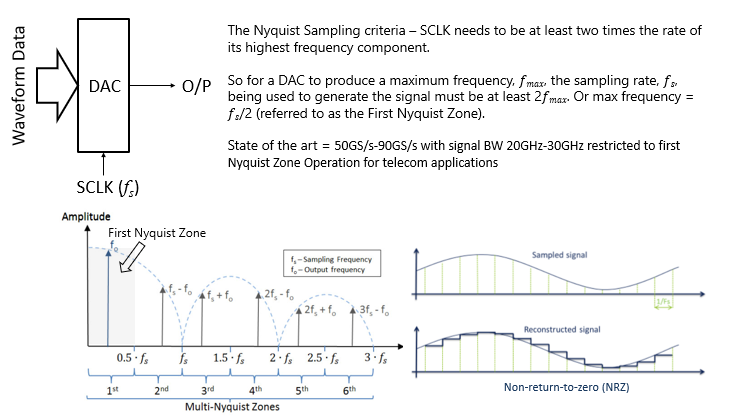
Figure 8c. Multiple Nyquist Zone Operation
When using multiple Nyquist zones one thing to pay attention to is spectral inversion. For example, in Figure 8d the sample clock is set to 2.5GS/s. Two frequency tones with 15dB’s of amplitude difference between are generated at around 1GHz – note the upper frequency tone has a lower amplitude than the lower frequency tone. The second Nyquist zone is at 2.5GS minus 1 GHz and the lower frequency tone now has a higher amplitude as the spectrum has been inverted. The third Nyquist Zone has inverted again at 3.5GS/s – so back to the original, non-spectrally inverted signal.
In theory, using multiple Nyquist zones could go on to infinity however a key specification in an instrument is the maximum analog bandwidth that is supported. For example; if input analog bandwidth rolls off at 4.5GHz then using my previous example at 2f+fc or 2 x 2.5GS/s + 1GHz puts the two tones at around 6GHz. In this case the amplitude roll-off
will be a combination of both the sin(x)/x roll off and the roll-off of the 4.5GHz input filter. The Proteus AWG has an option for a 9GHz input filter allowing multiple Nyquist zones and the Tabor SE5082 is used in applications up to 14GHz.
D. Digital IQ Modulation
If a DAC can create direct to RF signals, then an obvious next step is to embed a modulator into the device. The Proteus Arbitrary Waveform Generator has a complex mixer embedded within its architecture and is performance was demonstrated in the mixer section. Consider Figure 9d. The Internal FPGA routes the required signal from its 16GS memory to the IQ inputs of the DAC. The I and Q are mixed with the LO, which is provided by a Numerically Controlled Oscillator. This simplifies the creation of signals especially when we want to shape pulses considering a basic Transmon circuit on the lower part of the diagram. Traditionally a combination of an AWG mixing with a LO frequency would be used to create a specific pulse shape. The mixer is often an IQ mixer, which needs to be balanced and frequency nulled and is susceptible to temperature changes. Taking a digital approach simplifies the signal creation process considerably.


Figure 8d. Multiple Nyquist Zone Operation
Chapter Five – Frequency Planning
A. Moving carrier feed through, harmonics, clock signals out of band
Creating a spectrally pure signal requires some calculation and some experimentation to ensure that the desired frequency with modulation meets the control or measurement need. In a commercial instrument, multiple up and down conversion stages will be used to effectively move nonlinear, or spurious signals out of the band. This is often referred to as the frequency plan of the instrument.
B. Multistage conversion system
A typical multistage conversion system is shown in figure 9a. The first stage utilizes an IQ modulator, then a further two up-conversion stages with filter create the appropriate output frequency while minimizing spurious interference.

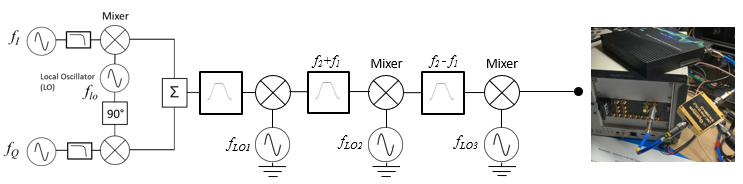
Figure 9a. Multistage conversion system
Referring to Figure 9b as an example - to produce two tones at 6.6GHz with limited Intermodulation. First, create a waveform in MATLAB with two tones centered around 1035MHz. This waveform has 4096 points and with the fast PCI data transfer of the Tabor Proteus unit can quickly upload this waveform and play it out. Then, using the internal IQ Modulator tuned to 2.2GHz amplitude, modulate the tones. In the second plot observe the 2.2 GHz carrier feedthrough and the tones spaces +/- 1035MHz on either side. Then, using a bandpass filter with a center frequency of the upper-sideband, feed that to an analog mixer with 4GHz of input bandwidth mixed with an LO signal of 3.4GHz. This example uses just the AM portion. Not the quadrature part. This provides an upper signal of 6.6GHz. Feedthrough will be at 3.4GHz and the lower sideband will be at 1.2GHz. Finally, use a high pass filter to ensure the feedthrough and lower sidebands are fully attenuated if required.

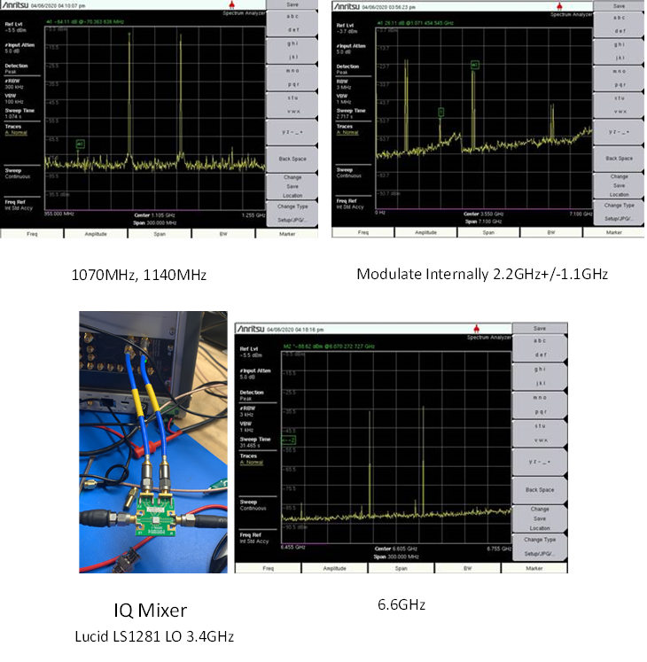
Figure 9b – Example of three stages of conversion
C. Experimentation and Trouble Shooting
This can all be achieved using relatively low cost commercially available connectorized components. As you can see there are no intermodulation products, but a couple of spurs 50dB down. The next exercise would be to determine if they are multiples of the DAC clocks, or are caused by the spectrum analyzer. To troubleshoot this, change the IQ modulator frequency and observe how the spurs behave in frequency. Or move the amplitude up and down to determine if they are due to nonlinear effects.
Chapter Six – Signal Analysis
A. Comparison of Analysis Techniques
For most RF signal measurements, a combination of Oscilloscope and Spectrum analyzer is used. Refer to Figure 10a. A spectrum analyzer sweeps a narrow bandwidth filter through a range of frequencies. The power displayed on the screen is the measured power in each sweep increment. As the filter is narrow the noise power is minimal, allowing for measurements with high sensitivity and a wide dynamic range. A variant of a spectrum analyzer is a Vector Signal Analyzer, this essentially works like a radio receiver. It does not sweep a range of frequencies but is tuned to a center frequency, then the bandwidth of the receiver filter is digitized and processed. The display could be a direct time domain representation of the acquired signal, or an FFT could be used to show the frequency range. As the filter is wider and the ADC sample rate is faster the noise and the spurious response of this type of architecture is not as good as the spectrum analyzer. But it can analyze signals with time domain behavior, namely modulated signals. An Oscilloscope or Digitizer is a broadband device. Its performance is defined by two specifications, its analog bandwidth, and its digitizer sample rate. In the example, the input bandwidth is limited to 1GHz by the analog BW, and the sample rate defines the spectral purity of the acquisition with a sample rate of 5 times the analog BW.


Figure 10a Comparison of RF analysis techniques
B. Choosing the correct analysis instrument
Spectrum analyzers have the best dynamic range and sensitivity so they are used when looking for spurious interference or measuring intermodulation products. If visualization and measurement of time domain phenomena are required, then an oscilloscope is the appropriate instrument. However, due to the wideband nature of an oscilloscope, the noise performance is limited. A compromise between the two instruments is a Vector Signal Analyzer or VSA.
C. Direct Digitization
In the previous diagram, the Oscilloscope had a filter that was lower in bandwidth than the sample clock. This filter could be omitted or made wider and as in the generation example, multiple Nyquist Zones could be used. For the advanced user this opens-up a whole new range of possibilities to use the instrument in multiple Nyquist's zones. This is called under sampling, however, the signal and the theory are the same as what we talked about in synthesis and utilizing multiple Nyquist zones. The Tabor Proteus digitizer allows this type of operation, providing cost effective high frequency digitization.


Figure 10b Direct Digitization
Conclusion
We have covered the fundamentals of wave propagation, understood the difference in wave velocities through a vacuum vs cables of different types and lengths, and gained an understanding of impendence matching and transmission lines to ensure maximum power transfer between two devices. In the second topic, we covered passive frequency translation and how the properties of nonlinear devices - namely diodes, configured as frequency multipliers or frequency summation devices such as mixers - can help modify the signal’s frequency. The Frequency Synthes Topic used many of the same principles as frequency translation and details how to convert a reference frequency to a desired frequency. Modulation and the process of encoding information on to generated frequency, using AM and Phase Modulation and how they are combined in a vector modulator, were covered. We examined both analog and digital implementations of modulation. We also learned about frequency planning or the optimization of the frequency translation path. To ensure that intermodulation and harmonic signals, do not interfere with the desired spectral purity of the desired signal we are trying to create a powerful tool. And finally, the topic of Signal Analysis and different analysis techniques and the benefits and trade-offs of each one should be understood.
For more information info@taborelec.com